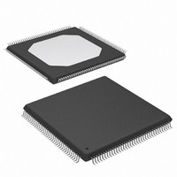
XC3S50-4TQG144C Xilinx Inc, XC3S50-4TQG144C Datasheet - Page 82

XC3S50-4TQG144C
Manufacturer Part Number
XC3S50-4TQG144C
Description
FPGA Spartan®-3 Family 50K Gates 1728 Cells 630MHz 90nm Technology 1.2V 144-Pin TQFP
Manufacturer
Xilinx Inc
Series
Spartan™-3r
Datasheet
1.XC3S50-4VQG100C.pdf
(217 pages)
Specifications of XC3S50-4TQG144C
Package
144TQFP
Family Name
Spartan®-3
Device Logic Units
1728
Device System Gates
50000
Maximum Internal Frequency
630 MHz
Typical Operating Supply Voltage
1.2 V
Maximum Number Of User I/os
97
Ram Bits
73728
Number Of Logic Elements/cells
1728
Number Of Labs/clbs
192
Total Ram Bits
73728
Number Of I /o
97
Number Of Gates
50000
Voltage - Supply
1.14 V ~ 1.26 V
Mounting Type
Surface Mount
Operating Temperature
0°C ~ 85°C
Package / Case
144-LQFP
Case
TQFP144
Dc
06+
Lead Free Status / RoHS Status
Lead free / RoHS Compliant
Available stocks
Company
Part Number
Manufacturer
Quantity
Price
Company:
Part Number:
XC3S50-4TQG144C
Manufacturer:
XILINX43
Quantity:
240
Part Number:
XC3S50-4TQG144C
Manufacturer:
XILINX/赛灵思
Quantity:
20 000
Spartan-3 FPGA Family: DC and Switching Characteristics
Internal Logic Timing
Table 50: CLB Timing
82
Notes:
1.
2.
3.
Clock-to-Output Times
T
Setup Times
T
T
Hold Times
T
T
Clock Timing
T
T
F
Propagation Times
T
Set/Reset Pulse Width
T
AS
AH
CKO
DICK
CKDI
CH
CL
TOG
ILO
RPW_CLB
The numbers in this table are based on the operating conditions set forth in
The timing shown is for SLICEM.
For minimums, use the values reported by the Xilinx timing analyzer.
Symbol
When reading from the FFX (FFY) Flip-Flop,
the time from the active transition at the CLK
input to data appearing at the XQ (YQ) output
Time from the setup of data at the F or G input
to the active transition at the CLK input of the
CLB
Time from the setup of data at the BX or BY
input to the active transition at the CLK input of
the CLB
Time from the active transition at the CLK input
to the point where data is last held at the F or
G input
Time from the active transition at the CLK input
to the point where data is last held at the BX or
BY input
CLB CLK signal High pulse width
CLB CLK signal Low pulse width
Maximum toggle frequency (for export control)
The time it takes for data to travel from the
CLB’s F (G) input to the X (Y) output
The minimum allowable pulse width, High or
Low, to the CLB’s SR input
Description
www.xilinx.com
0.46
1.27
0.25
0.69
0.76
0.69
Min
0
Table
-
-
-
-5
31.
Max
0.63
0.53
725
Speed Grade
∞
∞
-
-
-
-
-
DS099-3 (v2.5) December 4, 2009
0.53
1.57
0.29
0.79
0.79
0.87
Min
0
-
-
-
-4
Product Specification
Max
0.72
0.61
630
∞
∞
-
-
-
-
-
Units
MHz
ns
ns
ns
ns
ns
ns
ns
ns
ns
R


