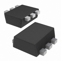
PBSS4220V,115 NXP Semiconductors, PBSS4220V,115 Datasheet - Page 4

PBSS4220V,115
Manufacturer Part Number
PBSS4220V,115
Description
TRANS NPN 20V 2A LOW SAT SOT666
Manufacturer
NXP Semiconductors
Series
-r
Datasheet
1.PBSS4220V115.pdf
(13 pages)
Specifications of PBSS4220V,115
Transistor Type
NPN
Current - Collector (ic) (max)
2A
Voltage - Collector Emitter Breakdown (max)
20V
Vce Saturation (max) @ Ib, Ic
350mV @ 200mA, 2A
Current - Collector Cutoff (max)
100nA
Dc Current Gain (hfe) (min) @ Ic, Vce
200 @ 1A, 2V
Power - Max
900mW
Frequency - Transition
210MHz
Mounting Type
Surface Mount
Package / Case
SS Mini-6 (SOT-666)
Lead Free Status / RoHS Status
Lead free / RoHS Compliant
Other names
934059259115
PBSS4220V T/R
PBSS4220V T/R
PBSS4220V T/R
PBSS4220V T/R
NXP Semiconductors
6. Thermal characteristics
PBSS4220V_2
Product data sheet
Fig 2.
Z
(K/W)
th(j-a)
10
10
10
10
−1
1
3
2
10
FR4 PCB, standard footprint
Transient thermal impedance from junction to ambient as a function of pulse time; typical values
−5
duty cycle =
1
0.5
0.2
0.1
0.05
0.02
0.01
0
0.75
0.33
10
−4
Table 6.
[1]
[2]
[3]
[4]
Symbol
R
R
th(j-a)
th(j-sp)
Device mounted on an FR4 PCB, single-sided copper, tin-plated and standard footprint.
Device mounted on an FR4 PCB, single-sided copper, tin-plated, mounting pad for collector 1 cm
Device mounted on a ceramic PCB, Al
Reflow soldering is the only recommended soldering method.
10
−3
Parameter
thermal resistance from
junction to ambient
thermal resistance from
junction to solder point
Thermal characteristics
10
Rev. 02 — 11 December 2009
−2
10
−1
2
O
3
, standard footprint.
Conditions
in free air
1
20 V, 2 A NPN low V
[1][4]
[2][4]
[3][4]
10
Min
-
-
-
-
PBSS4220V
CEsat
10
Typ
-
-
-
-
2
© NXP B.V. 2009. All rights reserved.
(BISS) transistor
t
p
006aaa425
(s)
Max
410
250
140
80
10
3
2
.
Unit
K/W
K/W
K/W
K/W
4 of 13


