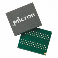
MT48LC4M32B2B5-7 IT:G Micron Technology Inc, MT48LC4M32B2B5-7 IT:G Datasheet - Page 63

MT48LC4M32B2B5-7 IT:G
Manufacturer Part Number
MT48LC4M32B2B5-7 IT:G
Description
DRAM Chip SDRAM 128M-Bit 4Mx32 3.3V 90-Pin VFBGA Tray
Manufacturer
Micron Technology Inc
Type
SDRAMr
Datasheet
1.MT48LC4M32B2P-7G_TR.pdf
(67 pages)
Specifications of MT48LC4M32B2B5-7 IT:G
Density
128 Mb
Maximum Clock Rate
143 MHz
Package
90VFBGA
Address Bus Width
14 Bit
Operating Supply Voltage
3.3 V
Maximum Random Access Time
17|8|5.5 ns
Operating Temperature
-40 to 85 °C
Format - Memory
RAM
Memory Type
SDRAM
Memory Size
128M (4Mx32)
Speed
143MHz
Interface
Parallel
Voltage - Supply
3 V ~ 3.6 V
Package / Case
90-VFBGA
Organization
4Mx32
Address Bus
14b
Access Time (max)
17/8/5.5ns
Operating Supply Voltage (typ)
3.3V
Package Type
VFBGA
Operating Temp Range
-40C to 85C
Operating Supply Voltage (max)
3.6V
Operating Supply Voltage (min)
3V
Supply Current
175mA
Pin Count
90
Mounting
Surface Mount
Operating Temperature Classification
Industrial
Lead Free Status / RoHS Status
Lead free / RoHS Compliant
Figure 46:
PDF: 09005aef80872800/Source: 09005aef80863355
128MbSDRAMx32_2.fm - Rev. L 1/09 EN
COMMAND
A0–A9, A11
BA0, BA1
DQM0–3
CLK
CKE
A10
DQ
t CMS
t CKS
t AS
t AS
t AS
ACTIVE
BANK 0
T0
ROW
ROW
Alternating Bank Write Accesses
t CKH
t CMH
t AH
t AH
t AH
t RCD - BANK 0
t RAS - BANK 0
t
t
RC - BANK 0
RRD
Notes:
t CK
T1
NOP
1. For this example, BL = 4.
2. Faster frequencies require two clocks (when
3. A8, A9, and A11 = “Don’t Care.”
ENABLE AUTO PRECHARGE
t CMS
t CL
COLUMN m 3
t DS
BANK 0
WRITE
T2
D
IN
t CMH
t CH
t DH
m
t DS
D
IN
T3
NOP
m + 1
t DH
t DS
D
BANK 1
ACTIVE
IN
T4
ROW
ROW
m + 2
t DH
63
t RCD - BANK 1
t DS
D
IN
T5
NOP
m + 3
t DH
Micron Technology, Inc., reserves the right to change products or specifications without notice.
t WR
ENABLE AUTO PRECHARGE
2
- BANK 0
t
COLUMN b 3
t DS
WR >
BANK 1
WRITE
T6
D
IN
t DH
b
t
CK).
t DS
D
NOP
T7
IN
b + 1
t DH
t RP - BANK 0
©2001 Micron Technology, Inc. All rights reserved.
128Mb: x32 SDRAM
t DS
D
Timing Diagrams
IN
NOP
T8
b + 2
t DH
t DS
D
BANK 0
ACTIVE
T9
ROW
IN
ROW
b + 3
t
t
RCD - BANK 0
WR - BANK 1
DON’T CARE
t DH


