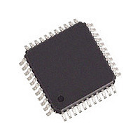
82V2081PPG8 IDT, Integrated Device Technology Inc, 82V2081PPG8 Datasheet - Page 9

82V2081PPG8
Manufacturer Part Number
82V2081PPG8
Description
Manufacturer
IDT, Integrated Device Technology Inc
Datasheet
1.82V2081PPG8.pdf
(68 pages)
Specifications of 82V2081PPG8
Number Of Transceivers
1
Screening Level
Industrial
Mounting
Surface Mount
Package Type
TQFP
Operating Temperature (min)
-40C
Operating Temperature (max)
85C
Lead Free Status / RoHS Status
Compliant
Notes:
1. TCLK missing: the state of TCLK continues to be high level or low level over 70 MCLK cycles.
SINGLE CHANNEL T1/E1/J1 LONG HAUL/SHORT HAUL LINE INTERFACE UNIT
2
Table-1 Pin Description
RD/RDP
CV/RDN
TD/TDP
RRING
TRING
Name
TCLK
RCLK
TTIP
RTIP
TDN
PIN DESCRIPTION
Analog
Analog
output
input
Type
O
O
I
I
Pin No.
37
36
41
40
2
3
1
5
6
4
TTIP/TRING: Transmit Bipolar Tip/Ring
These pins are the differential line driver outputs. They will be in high impedance state under the following conditions:
•
•
•
•
•
•
RTIP/RRING: Receive Bipolar Tip/Ring
These signals are the differential receiver inputs.
TD: Transmit Data
When the device is in single rail mode, the NRZ data to be transmitted is input on this pin. Data on TD pin is sampled into the
device on the active edge of TCLK and is encoded by AMI, HDB3 or B8ZS line code rules before being transmitted. In this
mode, TDN should be connected to ground.
TDP/TDN: Positive/Negative Transmit Data
When the device is in dual rail mode, the NRZ data to be transmitted for positive/negative pulse is input on these pins. Data
on TDP/TDN pin is sampled into the device on the active edge of TCLK. The line code in dual rail mode is as follows:
TCLK: Transmit Clock input
This pin inputs 1.544 MHz for T1/J1 mode or 2.048 MHz for E1 mode transmit clock. The transmit data at TD/TDP or TDN is
sampled into the device on the active edge of TCLK. If TCLK is missing
rupt will be generated.
RD: Receive Data output
In single rail mode, this pin outputs NRZ data. The data is decoded according to AMI, HDB3 or B8ZS line code rules.
CV: Code Violation indication
In single rail mode, the BPV/CV code violation will be reported by driving the CV pin to high level for a full clock cycle. B8ZS/
HDB3 line code violation can be indicated if the B8ZS/HDB3 decoder is enabled. When AMI decoder is selected, bipolar vio-
lation will be indicated.
In hardware control mode, the EXZ, BPV/CV errors in received data stream are always monitored by the CV pin if single rail
mode is chosen.
RDP/RDN: Positive/Negative Receive Data output
In dual rail mode, this pin outputs the re-timed NRZ data when CDR is enabled, or directly outputs the raw RZ slicer data if CDR
is bypassed.
Active edge and level select:
Data on RDP/RDN or RD is clocked with either the rising or the falling edge of RCLK. The active polarity is also selectable.
RCLK: Receive Clock output
This pin outputs 1.544 MHz for T1/J1 mode or 2.048 MHz for E1 mode receive clock. Under LOS condition with AIS enabled
(bit AISE=1), RCLK is derived from MCLK. In clock recovery mode, this signal provides the clock recovered from the RTIP/
RRING signal. The receive data (RD in single rail mode or RDP and RDN in dual rail mode) is clocked out of the device on the
active edge of RCLK. If clock recovery is bypassed, RCLK is the exclusive OR (XOR) output of the dual rail slicer data RDP
and RDN. This signal can be used in applications with external clock recovery circuitry.
THZ pin is high;
THZ bit is set to 1;
Loss of MCLK;
Loss of TCLK (exceptions: Remote Loopback; transmit internal pattern by MCLK);
Transmit path power down;
After software reset; pin reset and power on.
TDP
0
0
1
1
TDN
0
1
0
1
9
Space
Positive Pulse
Negative Pulse
Space
Output Pulse
Description
1
and the TCLK missing interrupt is not masked, an inter-
TEMPERATURE RANGES
INDUSTRIAL


