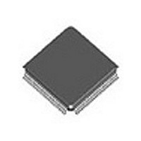
82V1074PF IDT, Integrated Device Technology Inc, 82V1074PF Datasheet - Page 51

82V1074PF
Manufacturer Part Number
82V1074PF
Description
Manufacturer
IDT, Integrated Device Technology Inc
Datasheet
1.82V1074PF.pdf
(107 pages)
Specifications of 82V1074PF
Number Of Channels
4
On-hook Transmission
Yes
Polarity Reversal
Yes
On-chip Ring Relay Driver
Yes
Operating Supply Voltage (typ)
3.3V
Operating Temp Range
-40C to 85C
Package Type
TQFP
Operating Temperature Classification
Industrial
Pin Count
100
Mounting
Surface Mount
Operating Current
95mA
Operating Supply Voltage (max)
3.465V
Operating Supply Voltage (min)
3.135V
Lead Free Status / RoHS Status
Not Compliant
- Current page: 51 of 107
- Download datasheet (2Mb)
4.1.2
linear code) is transferred through the PCM interface. The CODEC
provides two transmit and two receive PCM highways for all four
channels. The PCM interface consists of eight pins as shown below:
4.1.2.1
RSLIC & CODEC CHIPSET
In PCM/MPI mode, the PCM data (A/µ-law compressed code or
FSC:
BCLK:
DX1:
DR1:
TSX1:
DX2:
DR2:
TSX2:
The PCM interface is flexible with the data rate, clock slope and
PCM INTERFACE
PCM Clock Configuration
frame synchronization clock
PCM bit clock
PCM transmit data highway 1
PCM receive data highway 1
PCM data transmit indicator 1, active low
PCM transmit data highway 2
PCM receive data highway 2
PCM data transmit indicator 2, active low
(Double Clock Mode)
(Single Clock Mode)
BCLK
BCLK
FSC
Figure - 30 PCM Clock Slope Select Waveform
Time Slot 0
Bit 7
51
delay period programmable. As shown in
be the same as the BCLK (single clock mode) or half of it (double clock
mode). This is done by setting the DBL_CLK bit in register GREG3 to 0
and 1 respectively. The PCM clock slope is selected by the
TR_SLOPE[1:0] bits in register GREG3.
falling edge of the BCLK signal. If the BCLK signal is jitter free
PCM data can be received either on the rising edge or on the falling
edge. If the BCLK signal is not jitter free, please refer to the IDT82V1074
Application Note (AN-380) for details on the effective edge selection.
the FSC signal by 0 to 7 BCLK period(s). The PCM_OFT[2:0] bits in
GREG3 are used to set the offset period of the PCM timing.
The PCM data can be transmitted either on the rising edge or on the
The time slots for transmitting and receiving data can be offset from
1.Jitter free means that the BCLK signal is from an independent oscillator or a
system clock whose peak-to-peak jitter (> 4 kHz) is less than 0.01 UI.
Programmed by GREG3:
DBL_CLK = 0
TR_SLOPE[1:0] = 00
DBL_CLK = 0
TR_SLOPE[1:0] = 11
DBL_CLK = 1
TR_SLOPE[1:0] = 00
DBL_CLK = 1
TR_SLOPE[1:0] = 11
DBL_CLK = 0
TR_SLOPE[1:0] = 01
DBL_CLK = 0
TR_SLOPE[1:0] = 10
DBL_CLK = 1
TR_SLOPE[1:0] = 01
DBL_CLK = 1
TR_SLOPE[1:0] = 10
IDT82V1671/IDT82V1671A, IDT82V1074
Transmit
Receive
Figure -
30, the data rate can
1
, the
Related parts for 82V1074PF
Image
Part Number
Description
Manufacturer
Datasheet
Request
R

Part Number:
Description:
TRANSLATION DEVICE DPI 80-PQFP
Manufacturer:
IDT, Integrated Device Technology Inc
Datasheet:

Part Number:
Description:
IDT PART
Manufacturer:
IDT, Integrated Device Technology Inc
Datasheet:

Part Number:
Description:
IC LIU T1/E1/J1 OCTAL 256PBGA
Manufacturer:
IDT, Integrated Device Technology Inc
Datasheet:

Part Number:
Description:
IC FREQ TIMING GENERATOR 28TSSOP
Manufacturer:
IDT, Integrated Device Technology Inc
Datasheet:

Part Number:
Description:
IC CLK DVR PLL 1:10 40VFQFPN
Manufacturer:
IDT, Integrated Device Technology Inc
Datasheet:

Part Number:
Description:
IC CLK FANOUT BUFFER 1:18 32LQFP
Manufacturer:
IDT, Integrated Device Technology Inc
Datasheet:

Part Number:
Description:
IC CLK FANOUT BUFFER 1:18 32LQFP
Manufacturer:
IDT, Integrated Device Technology Inc
Datasheet:

Part Number:
Description:
IC CK505 VREG/RES 56TSSOP
Manufacturer:
IDT, Integrated Device Technology Inc
Datasheet:

Part Number:
Description:
IC SDRAM CLK DVR 1:10 48-TSSOP
Manufacturer:
IDT, Integrated Device Technology Inc
Datasheet:

Part Number:
Description:
IC CLK DVR PLL 1:10 48TSSOP
Manufacturer:
IDT, Integrated Device Technology Inc
Datasheet:

Part Number:
Description:
IC FLEXPC CLK PROGR P4 56-TSSOP
Manufacturer:
IDT, Integrated Device Technology Inc
Datasheet:

Part Number:
Description:
IC FLEXPC CLK PROGR P4 56-TSSOP
Manufacturer:
IDT, Integrated Device Technology Inc
Datasheet:

Part Number:
Description:
IC FLEXPC CLK PROGR P4 56-SSOP
Manufacturer:
IDT, Integrated Device Technology Inc
Datasheet:

Part Number:
Description:
IC PLL CLK DRIVER 2.5V 28-TSSOP
Manufacturer:
IDT, Integrated Device Technology Inc
Datasheet:

Part Number:
Description:
IC CLOCK DRIVER 2.5V 24-TSSOP
Manufacturer:
IDT, Integrated Device Technology Inc
Datasheet:


