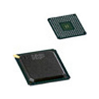
SAA7118E NXP Semiconductors, SAA7118E Datasheet - Page 13

SAA7118E
Manufacturer Part Number
SAA7118E
Description
Manufacturer
NXP Semiconductors
Datasheet
1.SAA7118E.pdf
(177 pages)
Specifications of SAA7118E
Adc/dac Resolution
9b
Screening Level
Commercial
Package Type
LBGA
Pin Count
156
Lead Free Status / RoHS Status
Compliant
Available stocks
Company
Part Number
Manufacturer
Quantity
Price
Part Number:
SAA7118E
Manufacturer:
PHILIPS/飞利浦
Quantity:
20 000
Company:
Part Number:
SAA7118E-V1
Manufacturer:
NXP
Quantity:
5 510
Company:
Part Number:
SAA7118E-V1
Manufacturer:
AD
Quantity:
5 510
Company:
Part Number:
SAA7118E/V1
Manufacturer:
PHI
Quantity:
480
Part Number:
SAA7118E/V1
Manufacturer:
PHILIPS/飞利浦
Quantity:
20 000
Company:
Part Number:
SAA7118E/V1,518
Manufacturer:
NXP Semiconductors
Quantity:
10 000
Company:
Part Number:
SAA7118E/V1,551
Manufacturer:
NXP Semiconductors
Quantity:
10 000
Company:
Part Number:
SAA7118E/V1,557
Manufacturer:
NXP Semiconductors
Quantity:
10 000
Part Number:
SAA7118E/V1/M5
Manufacturer:
PHILIPS/飞利浦
Quantity:
20 000
Company:
Part Number:
SAA7118E/V1/M5,518
Manufacturer:
Sigma Designs Inc
Quantity:
10 000
Company:
Part Number:
SAA7118EH
Manufacturer:
MNDSPEED
Quantity:
335
NXP Semiconductors
Table 4.
[1]
[2]
[3]
[4]
[5]
[6]
[7]
SAA7118_7
Product data sheet
Symbol
TDI
V
V
XTALI
XTALO
V
XTOUT
DNC9
DNC10
SSD13
SS(xtal)
DD(xtal)
I = input, O = output, P = power, NC = not connected, st = strapping, pu = pull-up, pd = pull-down, od = open-drain.
Pin strapping is done by connecting the pin to the supply via a 3.3 k resistor. During the power-up reset sequence the corresponding
pins are switched to input mode to read the strapping level. For the default setting no strapping resistor is necessary (internal pull-down).
Pin RTCO operates as I
Pin ALRCLK = LOW for 24.576 MHz crystal (default); pin ALRCLK = HIGH for 32.110 MHz crystal.
In accordance with the “IEEE1149.1” standard the pads TDI, TMS, TCK and TRST are input pads with an internal pull-up transistor and
TDO is a 3-state output pad.
For board design without boundary scan implementation connect the TRST pin to ground.
This pin provides easy initialization of the Boundary Scan Test (BST) circuit. TRST can be used to force the Test Access Port (TAP)
controller to the TEST_LOGIC_RESET state (normal operation) at once.
Pin description
Pin
QFP160
152
153
154
155
156
157
158
159
160
2
C-bus slave address pin; RTCO = 0 slave address 42h/43h (default); RTCO = 1 slave address 40h/41h.
LBGA156
B5
D5
A4
B4
A3
B3
A2
C3
C4
…continued
Type
I/pu
P
P
I
O
P
O
NC
NC
[1]
Rev. 07 — 7 July 2008
Description
test data input for boundary scan test
digital ground 13 (peripheral cells)
ground for crystal oscillator
input terminal for 24.576 MHz (32.11 MHz) crystal oscillator or
connection of external oscillator with TTL compatible square wave
clock signal
24.576 MHz (32.11 MHz) crystal oscillator output; not connected if
TTL clock input of XTALI is used
supply voltage for crystal oscillator
crystal oscillator output signal; auxiliary signal
do not connect, reserved for future extensions and for testing
do not connect, reserved for future extensions and for testing
Multistandard video decoder with adaptive comb filter
[5]
SAA7118
© NXP B.V. 2008. All rights reserved.
13 of 177


