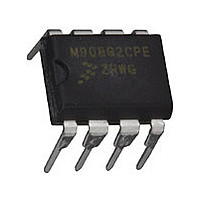
MC68HC908QT2CPE Freescale, MC68HC908QT2CPE Datasheet - Page 100

MC68HC908QT2CPE
Manufacturer Part Number
MC68HC908QT2CPE
Description
Manufacturer
Freescale
Datasheet
1.MC68HC908QT2CPE.pdf
(184 pages)
Specifications of MC68HC908QT2CPE
Cpu Family
HC08
Device Core Size
8b
Frequency (max)
8MHz
Total Internal Ram Size
128Byte
# I/os (max)
6
Number Of Timers - General Purpose
2
Operating Supply Voltage (typ)
3.3/5V
Operating Supply Voltage (max)
5.5V
Operating Supply Voltage (min)
2.7V
On-chip Adc
4-chx8-bit
Instruction Set Architecture
CISC
Operating Temp Range
-40C to 85C
Operating Temperature Classification
Industrial
Mounting
Through Hole
Pin Count
8
Package Type
PDIP
Program Memory Type
Flash
Program Memory Size
1.5KB
Lead Free Status / RoHS Status
Compliant
- Current page: 100 of 184
- Download datasheet (2Mb)
Input/Output Ports (PORTS)
PTAPUE[5:0] — Port A Input Pullup Enable Bits
12.3 Port B
Port B is an 8-bit general purpose I/O port. Port B is only available on the MC68HC908QY1,
MC68HC908QY2, and MC68HC908QY4.
12.3.1 Port B Data Register
The port B data register (PTB) contains a data latch for each of the eight port B pins.
PTB[7:0] — Port B Data Bits
100
Table 12-1
1. X = don’t care
2. I/O pin pulled to V
3. Writing affects data register, but does not affect input.
4. Hi-Z = high impedance
5. Output does not apply to PTA2
PTAPUE
These read/write bits are software programmable to enable pullup devices on port A pins.
These read/write bits are software programmable. Data direction of each port B pin is under the control
of the corresponding bit in data direction register B. Reset has no effect on port B data.
Bit
X
1
0
1 = Corresponding port A pin configured to have internal pull if its DDRA bit is set to 0
0 = Pullup device is disconnected on the corresponding port A pin regardless of the state of its
DDRA bit
summarizes the operation of the port A pins.
Address: $0001
DDRA
Reset:
Read:
Write:
Bit
0
0
1
DD
by internal pullup.
PTB7
Bit 7
PTA
X
Bit
X
X
(1)
Figure 12-5. Port B Data Register (PTB)
PTB6
MC68HC908QY/QT Family Data Sheet, Rev. 6
6
Input, V
Input, Hi-Z
Table 12-1. Port A Pin Functions
I/O Pin
Output
Mode
DD
PTB5
(2)
(4)
5
Unaffected by reset
PTB4
Accesses to DDRA
4
DDRA5–DDRA0
DDRA5–DDRA0
DDRA5–DDRA0
Read/Write
PTB3
3
PTB2
2
PTA5–PTA0
PTB1
Read
Pin
Pin
1
Accesses to PTA
Freescale Semiconductor
PTB0
Bit 0
PTA5–PTA0
PTA5–PTA0
PTA5–PTA0
Write
(3)
(3)
(5)
Related parts for MC68HC908QT2CPE
Image
Part Number
Description
Manufacturer
Datasheet
Request
R

Part Number:
Description:
TOWER ELEVATOR BOARDS HARDWARE
Manufacturer:
Freescale Semiconductor
Datasheet:

Part Number:
Description:
TOWER SERIAL I/O HARDWARE
Manufacturer:
Freescale Semiconductor
Datasheet:

Part Number:
Description:
LCD MODULE FOR TWR SYSTEM
Manufacturer:
Freescale Semiconductor
Datasheet:

Part Number:
Description:
DAUGHTER LCD WVGA I.MX51
Manufacturer:
Freescale Semiconductor
Datasheet:

Part Number:
Description:
TOWER SYSTEM BOARD MPC5125
Manufacturer:
Freescale Semiconductor
Datasheet:

Part Number:
Description:
KIT EVALUATION I.MX51
Manufacturer:
Freescale Semiconductor
Datasheet:

Part Number:
Description:
KIT DEVELOPMENT WINCE IMX25
Manufacturer:
Freescale Semiconductor
Datasheet:

Part Number:
Description:
TOWER SYSTEM KIT MPC5125
Manufacturer:
Freescale Semiconductor
Datasheet:

Part Number:
Description:
TOWER SYSTEM BOARD K40X256
Manufacturer:
Freescale Semiconductor
Datasheet:

Part Number:
Description:
TOWER SYSTEM KIT K40X256
Manufacturer:
Freescale Semiconductor
Datasheet:

Part Number:
Description:
Microcontrollers (MCU) MX28 PLATFORM DEV KIT
Manufacturer:
Freescale Semiconductor
Datasheet:

Part Number:
Description:
MCU, MPU & DSP Development Tools IAR KickStart Kit for Kinetis K60
Manufacturer:
Freescale Semiconductor
Datasheet:

Part Number:
Description:
24BIT HDMI MX535/08
Manufacturer:
Freescale Semiconductor
Datasheet:
Part Number:
Description:
Manufacturer:
Freescale Semiconductor, Inc
Datasheet:
Part Number:
Description:
Manufacturer:
Freescale Semiconductor, Inc
Datasheet:


