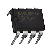
MC68HC908QT2CPE Freescale, MC68HC908QT2CPE Datasheet - Page 33

MC68HC908QT2CPE
Manufacturer Part Number
MC68HC908QT2CPE
Description
Manufacturer
Freescale
Datasheet
1.MC68HC908QT2CPE.pdf
(184 pages)
Specifications of MC68HC908QT2CPE
Cpu Family
HC08
Device Core Size
8b
Frequency (max)
8MHz
Total Internal Ram Size
128Byte
# I/os (max)
6
Number Of Timers - General Purpose
2
Operating Supply Voltage (typ)
3.3/5V
Operating Supply Voltage (max)
5.5V
Operating Supply Voltage (min)
2.7V
On-chip Adc
4-chx8-bit
Instruction Set Architecture
CISC
Operating Temp Range
-40C to 85C
Operating Temperature Classification
Industrial
Mounting
Through Hole
Pin Count
8
Package Type
PDIP
Program Memory Type
Flash
Program Memory Size
1.5KB
Lead Free Status / RoHS Status
Compliant
- Current page: 33 of 184
- Download datasheet (2Mb)
2.6 FLASH Memory (FLASH)
This subsection describes the operation of the embedded FLASH memory. The FLASH memory can be
read, programmed, and erased from a single external supply. The program and erase operations are
enabled through the use of an internal charge pump.
The FLASH memory consists of an array of 4096 or 1536 bytes with an additional 48 bytes for user
vectors. The minimum size of FLASH memory that can be erased is 64 bytes; and the maximum size of
FLASH memory that can be programmed in a program cycle is 32 bytes (a row). Program and erase
operations are facilitated through control bits in the FLASH control register (FLCR). Details for these
operations appear later in this section. The address ranges for the user memory and vectors are:
2.6.1 FLASH Control Register
The FLASH control register (FLCR) controls FLASH program and erase operations.
HVEN — High Voltage Enable Bit
MASS — Mass Erase Control Bit
Freescale Semiconductor
1. No security feature is absolutely secure. However, Freescale’s strategy is to make reading or copying the FLASH difficult
•
•
•
This read/write bit enables high voltage from the charge pump to the memory for either program or
erase operation. It can only be set if either PGM =1 or ERASE =1 and the proper sequence for
program or erase is followed.
This read/write bit configures the memory for mass erase operation.
for unauthorized users.
1 = High voltage enabled to array and charge pump on
0 = High voltage disabled to array and charge pump off
1 = Mass erase operation selected
0 = Mass erase operation unselected
$EE00 – $FDFF; user memory, 4096 bytes: MC68HC908QY4 and MC68HC908QT4
$F800 – $FDFF; user memory, 1536 bytes: MC68HC908QY2, MC68HC908QT2,
MC68HC908QY1 and MC68HC908QT1
$FFD0 – $FFFF; user interrupt vectors, 48 bytes.
Address:
An erased bit reads as a 1 and a programmed bit reads as a 0.
A security feature prevents viewing of the FLASH contents.
Reset:
Read:
Write:
$FE08
Bit 7
0
0
Figure 2-3. FLASH Control Register (FLCR)
= Unimplemented
MC68HC908QY/QT Family Data Sheet, Rev. 6
6
0
0
5
0
0
NOTE
4
0
0
HVEN
3
0
MASS
2
0
(1)
ERASE
1
0
FLASH Memory (FLASH)
PGM
Bit 0
0
33
Related parts for MC68HC908QT2CPE
Image
Part Number
Description
Manufacturer
Datasheet
Request
R

Part Number:
Description:
TOWER ELEVATOR BOARDS HARDWARE
Manufacturer:
Freescale Semiconductor
Datasheet:

Part Number:
Description:
TOWER SERIAL I/O HARDWARE
Manufacturer:
Freescale Semiconductor
Datasheet:

Part Number:
Description:
LCD MODULE FOR TWR SYSTEM
Manufacturer:
Freescale Semiconductor
Datasheet:

Part Number:
Description:
DAUGHTER LCD WVGA I.MX51
Manufacturer:
Freescale Semiconductor
Datasheet:

Part Number:
Description:
TOWER SYSTEM BOARD MPC5125
Manufacturer:
Freescale Semiconductor
Datasheet:

Part Number:
Description:
KIT EVALUATION I.MX51
Manufacturer:
Freescale Semiconductor
Datasheet:

Part Number:
Description:
KIT DEVELOPMENT WINCE IMX25
Manufacturer:
Freescale Semiconductor
Datasheet:

Part Number:
Description:
TOWER SYSTEM KIT MPC5125
Manufacturer:
Freescale Semiconductor
Datasheet:

Part Number:
Description:
TOWER SYSTEM BOARD K40X256
Manufacturer:
Freescale Semiconductor
Datasheet:

Part Number:
Description:
TOWER SYSTEM KIT K40X256
Manufacturer:
Freescale Semiconductor
Datasheet:

Part Number:
Description:
Microcontrollers (MCU) MX28 PLATFORM DEV KIT
Manufacturer:
Freescale Semiconductor
Datasheet:

Part Number:
Description:
MCU, MPU & DSP Development Tools IAR KickStart Kit for Kinetis K60
Manufacturer:
Freescale Semiconductor
Datasheet:

Part Number:
Description:
24BIT HDMI MX535/08
Manufacturer:
Freescale Semiconductor
Datasheet:
Part Number:
Description:
Manufacturer:
Freescale Semiconductor, Inc
Datasheet:
Part Number:
Description:
Manufacturer:
Freescale Semiconductor, Inc
Datasheet:


