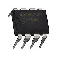
MC68HC908QT2CPE Freescale, MC68HC908QT2CPE Datasheet - Page 142

MC68HC908QT2CPE
Manufacturer Part Number
MC68HC908QT2CPE
Description
Manufacturer
Freescale
Datasheet
1.MC68HC908QT2CPE.pdf
(184 pages)
Specifications of MC68HC908QT2CPE
Cpu Family
HC08
Device Core Size
8b
Frequency (max)
8MHz
Total Internal Ram Size
128Byte
# I/os (max)
6
Number Of Timers - General Purpose
2
Operating Supply Voltage (typ)
3.3/5V
Operating Supply Voltage (max)
5.5V
Operating Supply Voltage (min)
2.7V
On-chip Adc
4-chx8-bit
Instruction Set Architecture
CISC
Operating Temp Range
-40C to 85C
Operating Temperature Classification
Industrial
Mounting
Through Hole
Pin Count
8
Package Type
PDIP
Program Memory Type
Flash
Program Memory Size
1.5KB
Lead Free Status / RoHS Status
Compliant
- Current page: 142 of 184
- Download datasheet (2Mb)
Development Support
The rising edge of the internal RST signal latches the monitor mode. Once monitor mode is latched, the
values on PTA1 and PTA4 pins can be changed.
Once out of reset, the MCU waits for the host to send eight security bytes (see
security bytes, the MCU sends a break signal (10 consecutive logic 0s) to the host, indicating that it is
ready to receive a command.
15.3.1.1 Normal Monitor Mode
RST and OSC1 functions will be active on the PTA3 and PTA5 pins respectively as long as V
applied to the IRQ pin. If the IRQ pin is lowered (no longer V
monitor mode, but the pin functions will be determined by the settings in the configuration registers (see
Chapter 5 Configuration Register
BIL instructions will read the IRQ pin state only if IRQEN is set in the CONFIG2 register.
142
Function
[Pin No.]
MON08
Monitor
Monitor
Normal
Forced
1. PTA0 must have a pullup resistor to V
2. Communication speed in the table is an example to obtain a baud rate of 9600. Baud rate using external oscillator is bus
3. External clock is a 9.8304 MHz oscillator on OSC1.
4. X = don’t care
5. MON08 pin refers to P&E Microcomputer Systems’ MON08-Cyclone 2 by 8-pin connector.
Mode
User
frequency / 256 and baud rate using internal oscillator is bus frequency / 335.
(PTA2)
V
V
IRQ
V
V
[6]
TST
TST
X
DD
SS
(PTA3)
RST
RST
V
[4]
X
X
X
DD
Table 15-1. Monitor Mode Signal Requirements and Options
Vector
(blank)
(blank)
$FFFF
$FFFF
$FFFF
Reset
Not
—
X
Communi-
MC68HC908QY/QT Family Data Sheet, Rev. 6
cation
Serial
PTA0
COM
(CONFIG)) when V
[8]
DD
OSC1
1
1
1
X
V
NC
NC
NC
NC
NC
NC
in monitor mode.
DD
MOD0
PTA1 PTA4
[12]
Selection
11
13
15
X
X
X
1
1
3
5
7
9
Mode
MOD1
[10]
10
12
14
16
X
X
X
0
2
4
6
8
TST
GND
RST
IRQ
PTA0
PTA4
PTA1
NC
NC
Disabled
Disabled
Disabled
Enabled
COP
—
was lowered. With V
TST
External
9.8304
9.8304
) then the chip will still be operating in
Clock
OSC1
MHz
MHz
[13]
X
X
Communication
Frequency
(Trimmed)
Speed
3.2 MHz
2.4576
2.4576
MHz
MHz
Bus
—
X
TST
15.3.2
lowered, the BIH and
Freescale Semiconductor
Baud
Rate
9600
9600
9600
—
Security). After the
X
Provide external
clock at OSC1.
Provide external
clock at OSC1.
Internal clock
is active.
Comments
TST
is
Related parts for MC68HC908QT2CPE
Image
Part Number
Description
Manufacturer
Datasheet
Request
R

Part Number:
Description:
TOWER ELEVATOR BOARDS HARDWARE
Manufacturer:
Freescale Semiconductor
Datasheet:

Part Number:
Description:
TOWER SERIAL I/O HARDWARE
Manufacturer:
Freescale Semiconductor
Datasheet:

Part Number:
Description:
LCD MODULE FOR TWR SYSTEM
Manufacturer:
Freescale Semiconductor
Datasheet:

Part Number:
Description:
DAUGHTER LCD WVGA I.MX51
Manufacturer:
Freescale Semiconductor
Datasheet:

Part Number:
Description:
TOWER SYSTEM BOARD MPC5125
Manufacturer:
Freescale Semiconductor
Datasheet:

Part Number:
Description:
KIT EVALUATION I.MX51
Manufacturer:
Freescale Semiconductor
Datasheet:

Part Number:
Description:
KIT DEVELOPMENT WINCE IMX25
Manufacturer:
Freescale Semiconductor
Datasheet:

Part Number:
Description:
TOWER SYSTEM KIT MPC5125
Manufacturer:
Freescale Semiconductor
Datasheet:

Part Number:
Description:
TOWER SYSTEM BOARD K40X256
Manufacturer:
Freescale Semiconductor
Datasheet:

Part Number:
Description:
TOWER SYSTEM KIT K40X256
Manufacturer:
Freescale Semiconductor
Datasheet:

Part Number:
Description:
Microcontrollers (MCU) MX28 PLATFORM DEV KIT
Manufacturer:
Freescale Semiconductor
Datasheet:

Part Number:
Description:
MCU, MPU & DSP Development Tools IAR KickStart Kit for Kinetis K60
Manufacturer:
Freescale Semiconductor
Datasheet:

Part Number:
Description:
24BIT HDMI MX535/08
Manufacturer:
Freescale Semiconductor
Datasheet:
Part Number:
Description:
Manufacturer:
Freescale Semiconductor, Inc
Datasheet:
Part Number:
Description:
Manufacturer:
Freescale Semiconductor, Inc
Datasheet:


