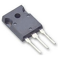
CMF10120D Cree Inc, CMF10120D Datasheet

CMF10120D
Specifications of CMF10120D
Related parts for CMF10120D
CMF10120D Summary of contents
Page 1
... AR I Repetitive Avalanche Current AR V Gate Source Voltage GS P Power Dissipation tot Operating Junction and Storage Temperature J stg T Solder Temperature L M Mounting Torque d 1 CMF10120D Rev DS(on Package TO-247-3 Part Number Package CMF10120D TO-247-3 Value Unit Test Conditions 24 V @20V 25˚ ...
Page 2
... Case to Sink, w/ Thermal Compound θCS R Thermal Resistance From Junction to Ambient θJA Gate Charge Characteristics Symbol Parameter Q Gate to Source Charge gs Q Gate to Drain Charge gd Q Gate Charge Total g 2 CMF10120D Rev. - Min. Typ. Max. Unit 1200 2.5 4 1.8 0 125 250 160 220 190 260 3.7 3 ...
Page 3
... 125 (V) GS Figure 3. Typical Transfer Characteristics 10000 10000 C 1000 1000 C 100 100 C rss 100 (V) DS Fig 5A and 5B. Typical Capacitance vs. Drain – Source Voltage 3 CMF10120D Rev =10V 25ºC Fig 2. Typical Output Characteristics T J ° Fig 4. Normalized On-Resistance vs. Temperature 10000 10000 MHz ...
Page 4
... Drain Current(A) Fig 7. Inductive Switching Energy(Turn-on) vs Gate Charge (nC) Fig 9. Typical Gate Charge Characteristics @ 25°C 4 CMF10120D Rev. - 100E-6 1E-3 10E-3 Time (sec -2/20V 11.8Ω Total 800V 10A Fig 8. Inductive Switching Energy(Turn-off 300 300 250 250 200 200 ...
Page 5
... Fig 11. Switching Waveform Test Circuit 10% Irr 10 Vpk Irr Diode Recovery Waveforms Erec= Diode Reverse Recovery Energy t1 t2 Fig 13. Body Diode Recovery Waveform 5 CMF10120D Rev GS(on) Input ( 10% V GS(off) C2D10120D 10A, 1200V SiC Schottky i D(on) CMF20120D D.U.T. Output ( D(off) trr ∫ Qrr ...
Page 6
... Fig 15. Avalanche Test Circuit Package Dimensions Package TO-247 CMF10120D Rev 1/ Fig 16. Theoretical Avalanche Waveform Inches POS Min Max A .190 .205 A1 .090 .100 A2 .075 .085 b .042 .052 b1 .075 .095 b2 .075 .085 b3 .113 .133 b4 .113 .123 c .022 .027 D .819 .831 D1 .640 .695 D2 .037 ...
Page 7
... Copyright © 2010-2011 Cree, Inc. All rights reserved. The information in this document is subject to change without notice. Cree and the Cree logo are registered trademarks and Z-REC and Z-FET are trademarks of Cree, Inc CMF10120D Rev. - TO-247-3 Part Number Package CMF10120D TO-247-3 Cree, Inc ...
Page 8
... Any excessive ringing that is present on the gate drive signal could cause unintentional turn-on or partial turn-off of the device. The gate resistance should be carefully selected to insure that the gate drive pulse is adequately dampened. To first order, the gate circuit can be approximated CMF10120D Rev. - needs to be 20V to optimize performance. This can GS /dt ≈ 0) until the V DS ...
Page 9
... The second stage is a small wide bandwidth current transformer, such as the Tektronix CT-2. Lastly, a separate source return should be used for the gate drive Tektronix CT-2. Lastly, a separate source return should be used for the gate drive as shown below: as shown below: 9 CMF10120D Rev LOOP C GATE ...
Page 10
... Therefore critical to manage the output interconnection parasitics (and snubbers) to keep the ringing and overshoot from becoming problematic. ESD RATINGS ESD Test ESD-HBM ESD-MM ESD-CDM 10 CMF10120D Rev. - Kelvin gate connection with separate source return is highly recommended LOAD CURRENT DRIVE LOAD CURRENT Total Devices Sampled All Devices Passed 1000V ...


