CMF10120D Cree Inc, CMF10120D Datasheet - Page 2
CMF10120D
Manufacturer Part Number
CMF10120D
Description
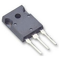
SIC MOSFET N-CH 1200V 24A TO247
Manufacturer
Cree Inc
Series
Z-FET™r
Specifications of CMF10120D
Fet Type
SiCFET N-Channel, Silicon Carbide
Fet Feature
Standard
Rds On (max) @ Id, Vgs
220 mOhm @ 10A, 20V
Drain To Source Voltage (vdss)
1200V (1.2kV)
Current - Continuous Drain (id) @ 25° C
24A
Vgs(th) (max) @ Id
4V @ 500µA
Gate Charge (qg) @ Vgs
47.1nC @ 20V
Input Capacitance (ciss) @ Vds
928pF @ 800V
Power - Max
152W
Mounting Type
*
Package / Case
*
Transistor Polarity
N Channel
Continuous Drain Current Id
24A
Drain Source Voltage Vds
1.2kV
On Resistance Rds(on)
0.16ohm
Rds(on) Test Voltage Vgs
20V
Rohs Compliant
YES
Configuration
Single
Resistance Drain-source Rds (on)
160 mOhms
Forward Transconductance Gfs (max / Min)
3.7 S, 3.4 S
Drain-source Breakdown Voltage
1200 V
Gate-source Breakdown Voltage
25 V
Continuous Drain Current
24 A
Power Dissipation
152 W
Mounting Style
Through Hole
Gate Charge Qg
47.1 nC
Lead Free Status / Rohs Status
Lead free / RoHS Compliant


NOTES: 1. The recommended on-state V
Reverse Diode Characteristics
Gate Charge Characteristics
Electrical Characteristics
Thermal Characteristics
Symbol
2
Symbol
Symbol
Symbol
V
R
V
t
t
(BR)DSS
I
I
C
C
C
d(off)i
E
E
GS(th)
DS(on)
d(on)i
R
g
R
R
R
Q
Q
DSS
GSS
V
I
t
t
Q
Q
t
oss
rss
ON
Off
iss
fi
rrm
θCS
fs
r
θJC
θJA
G
rr
gd
sd
gs
rr
g
CMF10120D Rev. -
Drain-Source Breakdown Voltage
Gate Threshold Voltage
Zero Gate Voltage Drain Current
Gate-Source Leakage Current
Drain-Source On-State Resistance
Transconductance
Input Capacitance
Output Capacitance
Reverse Transfer Capacitance
Turn-On Delay Time
Rise Time
Turn-Off Delay Time
Fall Time
Turn-On Switching Loss
Turn-Off Switching Loss
Internal Gate Resistance
Parameter
Thermal Resistance from Junction to Case
Case to Sink, w/ Thermal Compound
Thermal Resistance From Junction to Ambient
Parameter
Gate to Source Charge
Gate to Drain Charge
Gate Charge Total
Parameter
Diode Forward Voltage
Reverse Recovery Time
Reverse Recovery Charge
Peak Reverse Recovery Current
Parameter
GS
is +20V and the recommended off-state V
Min.
1200
Typ.
1.57
138
3.5
3.1
94
Typ.
11.8
21.5
47.1
Typ.
0.66
0.25
Typ.
7.45
13.6
160
190
928
261
120
2.5
1.8
0.5
3.7
3.4
63
14
46
37
Max.
5
7
Max.
Max.
40
Max. Unit
Unit
125
250
220
260
50
nC
ns
4
V
A
Unit
°C/W
Unit
mΩ
V
V
V
V
di
μA
nA
pF
ns
μJ
μJ
nC
Ω
V
V
S
GS
GS
GS
R
GS
F
/dt= 100A/μs
= 800V,
= -5V, I
= -2V, I
= -5V, I
is between -2V and -5V
V
V
V
V
V
V
V
V
V
V
V
V
f = 1MHz
V
V
V
I
R
L = 856μH
Per JEDEC24 Page 27
V
D
V
I
V
GS
DS
DS
DS
DS
GS
GS
GS
DS
DS
GS
DS
AC
DD
GS
G
GS
D
= 6.8Ω
DD
GS
= 10A
= 20V, I
= 20V, I
Test Conditions
= 25mV
= -5V, I
= V
= V
= 1200V, V
= 1200V, V
= 800V
= 20V, V
= 20V, I
= 20V, I
= 0V
= 800V
= -2/20V
= 0V, f = 1MHz , V
=10A
= 800V
= -2/20V Per JEDEC24-2
F
F
F
= 5A, T
= 5A, T
= 10A, T
GS
GS
Test Conditions
Test Conditions
Test Conditions
, I
, I
DS
DS
D
D
D
D
D
= 50μA
DS
J
J
= 500uA, T
= 500uA, T
= 10A, T
= 10A, T
= 10A, T
= 10A, T
= 25ºC
= 25ºC
J
= 0V
GS
GS
= 25ºC
= 0V, T
= 0V, T
J
J
AC
J
J
= 25ºC
= 125ºC
= 25ºC
= 125ºC
= 25mV
J
J
J
J
= 25ºC
= 125ºC
= 25ºC
= 125ºC
fig. 13,14
Note
fig. 4
fig. 3
fig. 5
fig. 12
fig. 6
Note
fig.9
Note
Note
1
Related parts for CMF10120D
Image
Part Number
Description
Manufacturer
Datasheet
Request
R

Part Number:
Description:
CREE PLCC4 SMD LED WHITE
Manufacturer:
Cree Inc
Datasheet:
Part Number:
Description:
CREE PLCC4 SMD LED WHITE
Manufacturer:
Cree Inc
Datasheet:

Part Number:
Description:
CREE PLCC4 SMD LED WHITE
Manufacturer:
Cree Inc
Datasheet:
Part Number:
Description:
CREE PLCC4 SMD LED WHITE
Manufacturer:
Cree Inc
Datasheet:
Part Number:
Description:
CREE PLCC4 SMD LED WHITE
Manufacturer:
Cree Inc
Datasheet:

Part Number:
Description:
DIODE SCHOTTKY 600V 16.5A TO-247
Manufacturer:
Cree Inc
Datasheet:

Part Number:
Description:
DIODE SCHOTTKY 600V 6A TO220-2
Manufacturer:
Cree Inc
Datasheet:
Part Number:
Description:
DIODE SCHOTTKY 600V 10A TO220-2
Manufacturer:
Cree Inc
Datasheet:

Part Number:
Description:
IC AMP MMIC HEMT 25W 780019PKG
Manufacturer:
Cree Inc
Datasheet:

Part Number:
Description:
Cree� XLamp� XT-E LEDs
Manufacturer:
CREE [Cree, Inc]
Datasheet:
Part Number:
Description:
Cree� EZBright290� LEDs
Manufacturer:
CREE [Cree, Inc]
Datasheet:

Part Number:
Description:
DIODE SCHOT 600V 2A ZREC TO220
Manufacturer:
Cree Inc
Datasheet:
Part Number:
Description:
DIODE SCHOT 600V 3A ZREC TO252
Manufacturer:
Cree Inc
Datasheet: