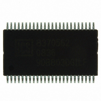
ICS9DB803DGILFT IDT, Integrated Device Technology Inc, ICS9DB803DGILFT Datasheet

ICS9DB803DGILFT
Specifications of ICS9DB803DGILFT
9DB803DGILFT
Available stocks
Related parts for ICS9DB803DGILFT
ICS9DB803DGILFT Summary of contents
Page 1
Eight Output Differential Buffer for PCIe Gen 2 Description The 9DB803 is a DB800 Version 2.0 Yellow Cover part with PCI Express Gen II support. It can be used embedded systems to provide outputs that have low ...
Page 2
ICS9DB803DI Eight Output Differential Buffer for PCIe for Gen 2 Pin Configuration SRC_DIV# 1 VDD 2 GND 3 SRC_IN 4 SRC_IN# 5 OE_0 6 OE_3 7 DIF_0 8 DIF_0# 9 GND 10 VDD 11 DIF_1 12 DIF_1# 13 OE_1 14 ...
Page 3
ICS9DB803DI Eight Output Differential Buffer for PCIe for Gen 2 Pin Description for OE_INV = 0 PIN # PIN NAME PIN TYPE 1 SRC_DIV VDD PWR 3 GND PWR 4 SRC_IN IN 5 SRC_IN OE_0 IN ...
Page 4
ICS9DB803DI Eight Output Differential Buffer for PCIe for Gen 2 Pin Description for OE_INV = 0 PIN # PIN NAME PIN TYPE 25 GND PWR 26 PD DIF_STOP HIGH_BW# PWR 29 DIF_4# OUT 30 DIF_4 OUT ...
Page 5
ICS9DB803DI Eight Output Differential Buffer for PCIe for Gen 2 Pin Description for OE_INV = 1 PIN # PIN NAME PIN TYPE 1 SRC_DIV# 2 VDD 3 GND 4 SRC_IN 5 SRC_IN# 6 OE0# 7 OE3# 8 DIF_0 9 DIF_0# ...
Page 6
ICS9DB803DI Eight Output Differential Buffer for PCIe for Gen 2 Pin Description for OE_INV = 1 PIN # PIN NAME PIN TYPE 25 GND DIF_STOP 28 HIGH_BW# 29 DIF_4# 30 DIF_4 31 VDD 32 GND 33 DIF_5# ...
Page 7
ICS9DB803DI Eight Output Differential Buffer for PCIe for Gen 2 Absolute Max Symbol Parameter VDD_A 3.3V Core Supply Voltage VDD_In 3.3V Logic Supply Voltage V Input Low Voltage IL V Input High Voltage IH Ts Storage Temperature Tambient Ambient Operating ...
Page 8
ICS9DB803DI Eight Output Differential Buffer for PCIe for Gen 2 Electrical Characteristics - Clock Input Parameters T = -40 - 85°C; Supply Voltage PARAMETER SYMBOL Input High Voltage - V IHDIF DIF_IN Input Low Voltage - V ...
Page 9
ICS9DB803DI Eight Output Differential Buffer for PCIe for Gen 2 Electrical Characteristics - DIF 0.7V Current Mode Differential Pair T = -40 - 85° 3.3 V +/-5 PARAMETER SYMBOL Current Source Output Zo Impedance ...
Page 10
ICS9DB803DI Eight Output Differential Buffer for PCIe for Gen 2 Clock Periods Differential Outputs with Spread Spectrum Enabled Measurement Window 1 Clock Symbol Lg- Absolute Short-term Period Average Definition Minimum Minimum Absolute Absolute Period Period 9.87400 9.99900 DIF 100 7.41425 ...
Page 11
ICS9DB803DI Eight Output Differential Buffer for PCIe for Gen 2 Common Recommendations for Differential Routing L1 length, Route as non-coupled 50 ohm trace. L2 length, Route as non-coupled 50 ohm trace. L3 length, Route as non-coupled 50 ohm trace. Rs ...
Page 12
ICS9DB803DI Eight Output Differential Buffer for PCIe for Gen 2 Alternative termination for LVDS and other common differential signals. Vdiff Vp-p Vcm 0.45 v 0.22v 1.08 0.58 0.28 0.6 0.80 0.40 0.6 0.60 0.3 1.2 R1a = R1b = R1 ...
Page 13
ICS9DB803DI Eight Output Differential Buffer for PCIe for Gen 2 General SMBus serial interface information for the ICS9DB803DI How to Write: • Controller (host) sends a start bit. • Controller (host) sends the write address DC • ICS clock will ...
Page 14
ICS9DB803DI Eight Output Differential Buffer for PCIe for Gen 2 SMBus Table: Frequency Select Register, READ/WRITE ADDRESS (DC/DD) Byte 0 Pin # Name Bit 7 - PD_Mode Bit 6 - STOP_Mode Bit 5 - PD_Polarity Bit 4 - Reserved Bit ...
Page 15
ICS9DB803DI Eight Output Differential Buffer for PCIe for Gen 2 SMBus Table: Vendor & Revision ID Register Byte 4 Pin # Name - RID3 Bit 7 - RID2 Bit 6 - RID1 Bit 5 - RID0 Bit 4 - VID3 ...
Page 16
ICS9DB803DI Eight Output Differential Buffer for PCIe for Gen 2 Note: Polarities in timing diagrams are shown OE_INV = 0. They are similar to OE_INV = 1. PD#, Power Down The PD# pin cleanly shuts off all clocks and places ...
Page 17
ICS9DB803DI Eight Output Differential Buffer for PCIe for Gen 2 SRC_STOP# The SRC_STOP# signal is an active-low asynchronous input that cleanly stops and starts the DIF outputs. A valid clock must be present on SRC_IN for this input to work ...
Page 18
ICS9DB803DI Eight Output Differential Buffer for PCIe for Gen 2 SRC_STOP_3 (SRC_Stop = Driven Tristate) SRC_Stop# PWRDWN# DIF (Free Running) DIF# (Free Running) DIF (Stoppable) DIF# (Stoppable) SRC_STOP_4 (SRC_Stop = Tristate Tristate) SRC_Stop# PWRDWN# DIF (Free ...
Page 19
ICS9DB803DI Eight Output Differential Buffer for PCIe for Gen INDEX INDEX AREA AREA 45° Ordering Information ICS9DB803DFILFT Example: ICS XXXX Eight Output ...
Page 20
... ICS9DB803DI Eight Output Differential Buffer for PCIe for Gen INDEX INDEX AREA AREA Ordering Information ICS9DB803DGILFT Example: ICS XXXX Eight Output Differential Buffer for PCIe Gen IDT /ICS c L SYMBOL aaa VARIATIONS Reference Doc.: JEDEC Publication 95, MO-153 SEATING SEATING PLANE PLANE ...
Page 21
ICS9DB803DI Eight Output Differential Buffer for PCIe Gen 2 Revision History Rev. Issue Date Description 0.1 6/18/2008 1. Initial Release TM Innovate with IDT and accelerate your future networks. Contact: www.IDT.com For Sales For Tech Support 800-345-7015 408-284-6578 408-284-8200 pcclockhelp@idt.com ...


