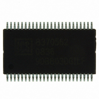
ICS9DB803DGILFT IDT, Integrated Device Technology Inc, ICS9DB803DGILFT Datasheet - Page 3

ICS9DB803DGILFT
Manufacturer Part Number
ICS9DB803DGILFT
Description
IC BUFFER 8OUTPUT DIFF 48-TSSOP
Manufacturer
IDT, Integrated Device Technology Inc
Type
Clock Bufferr
Datasheet
1.ICS9DB803DGILFT.pdf
(21 pages)
Specifications of ICS9DB803DGILFT
Input
HCSL
Output
HCSL, LVDS
Frequency - Max
400MHz
Voltage - Supply
3.135 V ~ 3.465 V
Operating Temperature
-40°C ~ 85°C
Mounting Type
Surface Mount
Package / Case
48-TSSOP
Frequency-max
400MHz
Lead Free Status / RoHS Status
Lead free / RoHS Compliant
Other names
800-1251-2
9DB803DGILFT
9DB803DGILFT
Available stocks
Company
Part Number
Manufacturer
Quantity
Price
Part Number:
ICS9DB803DGILFT
Manufacturer:
IDT
Quantity:
20 000
Pin Description for OE_INV = 0
IDT
PIN #
10
11
12
13
14
15
16
17
18
19
20
21
22
23
24
ICS9DB803DI
Eight Output Differential Buffer for PCIe for Gen 2
1
2
3
4
5
6
7
8
9
TM
/ICS
SRC_DIV#
VDD
GND
SRC_IN
SRC_IN#
OE_0
OE_3
DIF_0
DIF_0#
GND
VDD
DIF_1
DIF_1#
OE_1
OE_2
DIF_2
DIF_2#
GND
VDD
DIF_3
DIF_3#
BYPASS#/PLL
SCLK
SDATA
TM
PIN NAME
Eight Output Differential Buffer for PCIe Gen 2
PIN TYPE
PWR
PWR
PWR
PWR
PWR
PWR
OUT
OUT
OUT
OUT
OUT
OUT
OUT
OUT
I/O
IN
IN
IN
IN
IN
IN
IN
IN
IN
Active low Input for determining SRC output frequency SRC or SRC/2.
0 = SRC/2, 1= SRC
Power supply, nominal 3.3V
Ground pin.
0.7 V Differential SRC TRUE input
0.7 V Differential SRC COMPLEMENTARY input
Active high input for enabling output 0.
0 = tri-state outputs, 1= enable outputs
Active high input for enabling output 3.
0 = tri-state outputs, 1= enable outputs
0.7V differential true clock output
0.7V differential complement clock output
Ground pin.
Power supply, nominal 3.3V
0.7V differential true clock output
0.7V differential complement clock output
Active high input for enabling output 1.
0 = tri-state outputs, 1= enable outputs
Active high input for enabling output 2.
0 = tri-state outputs, 1= enable outputs
0.7V differential true clock output
0.7V differential complement clock output
Ground pin.
Power supply, nominal 3.3V
0.7V differential true clock output
0.7V differential complement clock output
Input to select Bypass(fan-out) or PLL (ZDB) mode
0 = Bypass mode, 1= PLL mode
Clock pin of SMBus circuitry, 5V tolerant.
Data pin for SMBus circuitry, 5V tolerant.
3
DESCRIPTION
ICS9DB803DI
REV A 06/18/08


