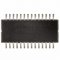
MK74CB218RLFTR IDT, Integrated Device Technology Inc, MK74CB218RLFTR Datasheet - Page 2

MK74CB218RLFTR
Manufacturer Part Number
MK74CB218RLFTR
Description
IC CLOCK DRIVER DUAL 1-8 28-SSOP
Manufacturer
IDT, Integrated Device Technology Inc
Series
74CB, Buffalo™r
Type
Fanout Buffer (Distribution)r
Datasheet
1.MK74CB218RLFTR.pdf
(7 pages)
Specifications of MK74CB218RLFTR
Number Of Circuits
2
Ratio - Input:output
1:8
Differential - Input:output
No/No
Input
LVCMOS
Output
LVCMOS
Frequency - Max
200MHz
Voltage - Supply
3 V ~ 3.6 V
Operating Temperature
0°C ~ 70°C
Mounting Type
Surface Mount
Package / Case
28-SSOP
Frequency-max
200MHz
Number Of Outputs
16
Operating Supply Voltage (max)
3.6V
Operating Temp Range
0C to 70C
Propagation Delay Time
20ns
Operating Supply Voltage (min)
3V
Mounting
Surface Mount
Pin Count
28
Operating Supply Voltage (typ)
3.3V
Package Type
QSOP
Input Frequency
200MHz
Duty Cycle
60%
Operating Temperature Classification
Commercial
Lead Free Status / RoHS Status
Lead free / RoHS Compliant
Other names
800-1880-2
Pin Assignment
Pin Descriptions
IDT™ / ICS™ DUAL 1 TO 8 BUFFALO™ CLOCK DRIVER
11, 12, 13 QA5, QA6, QA7 Output Clock A outputs.
16, 17, 18 QB7, QB6, QB5 Output Clock B outputs.
25, 26, 27 QB2, QB1, QB0 Output Clock B outputs.
Number
MK74CB218
DUAL 1 TO 8 BUFFALO™ CLOCK DRIVER
2, 3, 4
19, 20
21, 22
23, 24
9, 10
Pin
5, 6
7, 8
14
15
28
1
VDDA
VDDA
GND
GND
QA0
QA1
QA2
QA3
QA4
QA5
QA6
QA7
QA0, QA1, QA2 Output Clock A outputs.
INA
OE
QA3, QA4
QB4, QB3
Name
VDDA
VDDB
GND
GND
VDD
Pin
INA
INB
OE
1
2
3
4
5
6
7
8
9
10
11
12
13
14
Output Clock A outputs.
Output Clock B outputs.
Power
Power
Power
Power
Power
Type
Input
Input
Input
Pin
28
27
26
25
24
23
22
21
20
19
18
17
16
15
Clock input for eight A outputs.
Power supply for QA outputs. Connect to a voltage from 2.5 V to VDD. Cannot exceed
VDD.
Connect to ground.
Output Enable. Tri-states all clock outputs when this input is low. Internal pull-up to VDD.
Power supply for inputs.
Connect to ground.
Power supply for QB outputs. Connect to a voltage from 2.5 V to VDD. Cannot exceed
VDD.
Clock input for eight B outputs.
INB
QB0
QB1
QB2
VDDB
VDDB
QB3
QB4
GND
GND
QB5
QB6
QB7
VDD
2
Suggested Layout
0.01 µF
Pin Description
NOTE: 33 ohm series termination resistors for each output are
essential for operation.
For simplicity, series termination resistors are not shown for
the outputs, but should be placed as close to the device as
possible. It is most critical to have the 0.01 µF decoupling
capacitors closest.
A
V
G
A
= connect to VDDA
= connect to VDD
G
B
MK74CB218
= connect to VDDB
= connect to low
inductance ground plane
FAN OUT BUFFER
V
0.01 µF
0.01 µF
G
REV K 051310
B
G


