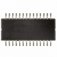
MK74CB218RLFTR IDT, Integrated Device Technology Inc, MK74CB218RLFTR Datasheet - Page 4

MK74CB218RLFTR
Manufacturer Part Number
MK74CB218RLFTR
Description
IC CLOCK DRIVER DUAL 1-8 28-SSOP
Manufacturer
IDT, Integrated Device Technology Inc
Series
74CB, Buffalo™r
Type
Fanout Buffer (Distribution)r
Datasheet
1.MK74CB218RLFTR.pdf
(7 pages)
Specifications of MK74CB218RLFTR
Number Of Circuits
2
Ratio - Input:output
1:8
Differential - Input:output
No/No
Input
LVCMOS
Output
LVCMOS
Frequency - Max
200MHz
Voltage - Supply
3 V ~ 3.6 V
Operating Temperature
0°C ~ 70°C
Mounting Type
Surface Mount
Package / Case
28-SSOP
Frequency-max
200MHz
Number Of Outputs
16
Operating Supply Voltage (max)
3.6V
Operating Temp Range
0C to 70C
Propagation Delay Time
20ns
Operating Supply Voltage (min)
3V
Mounting
Surface Mount
Pin Count
28
Operating Supply Voltage (typ)
3.3V
Package Type
QSOP
Input Frequency
200MHz
Duty Cycle
60%
Operating Temperature Classification
Commercial
Lead Free Status / RoHS Status
Lead free / RoHS Compliant
Other names
800-1880-2
Absolute Maximum Ratings
DC Electrical Characteristics
IDT™ / ICS™ DUAL 1 TO 8 BUFFALO™ CLOCK DRIVER
Operating Voltage
Operating Voltage
Operating Supply Current
Input High Voltage
Input Low Voltage
Input High Voltage
Input Low Voltage
Output High Voltage
Output High Voltage
Output Low Voltage
Output High Voltage
Output Low Voltage
Output Impedance
Short Circuit Current
Input Capacitance
On-chip Pull-up Resistor
MK74CB218
DUAL 1 TO 8 BUFFALO™ CLOCK DRIVER
Stresses above the ratings listed below can cause permanent damage to the MK74CB218. These ratings, which
are standard values for IDT commercially rated parts, are stress ratings only. Functional operation of the device at
these or any other conditions above those indicated in the operational sections of the specifications is not implied.
Exposure to absolute maximum rating conditions for extended periods can affect product reliability. Electrical
parameters are guaranteed only over the recommended operating temperature range.
Unless stated otherwise, VDD = 3.3 V ±10%
Note: Short circuits may be applied indefintely, but only one output may be shorted at a time to prevent exceeding
the power dissipation rating of this package.
Parameter
Supply Voltage, VDD (referenced to GND)
All Inputs and Outputs (referenced to GND)
Ambient Operating Temperature
Storage Temperature
Soldering Temperature
VDDA or VDDB
Symbol
Item
VDD
V
V
V
R
IDD
V
V
V
V
C
V
V
OH
OH
OH
OL
OL
PU
IH
IH
IN
IL
IL
At 100 MHz, No load
INA, INB pins
INA, INB pins
OE pin
OE pin
I
I
I
VDD = 2.5 V,
I
VDD = 2.5 V,
I
Each output,
VOUT=GND or VDD
OE
OH
OH
OL
OH
OL
= 25 mA
= 16 mA
= -12 mA
= -25 mA
= -16 mA
Conditions
4
5.2 V
-0.5 V to VDD+0.5 V
0 to +70 C
-65 C to 150 C
260 C (max. of 20 seconds)
0.65VDD
VDD-0.4
2.375
Min.
3.0
2.0
2.4
2
Typ.
Rating
100
250
3.3
75
14
7
0.35VDD
Max.
VDD
MK74CB218
3.6
0.8
0.8
0.5
FAN OUT BUFFER
Units
mA
mA
pF
k
V
V
V
V
V
V
V
V
V
V
V
REV K 051310


