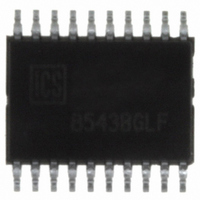
ICS8543BGLF IDT, Integrated Device Technology Inc, ICS8543BGLF Datasheet - Page 2

ICS8543BGLF
Manufacturer Part Number
ICS8543BGLF
Description
IC FANOUT BUFF DIFF-LVDS 20TSSOP
Manufacturer
IDT, Integrated Device Technology Inc
Type
Fanout Buffer (Distribution), Multiplexerr
Series
HiPerClockS™r
Datasheet
1.ICS8543BGLF.pdf
(18 pages)
Specifications of ICS8543BGLF
Number Of Circuits
1
Ratio - Input:output
2:4
Differential - Input:output
Yes/Yes
Input
CML, HCSL, LVDS, LVHSTL, LVPECL, SSTL
Output
LVDS
Frequency - Max
800MHz
Voltage - Supply
3.135 V ~ 3.465 V
Operating Temperature
0°C ~ 70°C
Mounting Type
Surface Mount
Package / Case
20-TSSOP
Frequency-max
800MHz
Number Of Clock Inputs
2
Mode Of Operation
Differential
Output Frequency
800MHz
Output Logic Level
LVDS
Operating Supply Voltage (min)
3.135V
Operating Supply Voltage (typ)
3.3V
Operating Supply Voltage (max)
3.465V
Package Type
TSSOP
Operating Temp Range
0C to 70C
Operating Temperature Classification
Commercial
Mounting
Surface Mount
Pin Count
20
Lead Free Status / RoHS Status
Lead free / RoHS Compliant
Other names
800-1186
800-1186-5
800-1186
8543BGLF
800-1186-5
800-1186
8543BGLF
Available stocks
Company
Part Number
Manufacturer
Quantity
Price
Company:
Part Number:
ICS8543BGLF
Manufacturer:
IDT
Quantity:
755
Part Number:
ICS8543BGLFT
Manufacturer:
IDT
Quantity:
20 000
ICS8543 Data Sheet
Table 1. Pin Descriptions
NOTE: Pullup and Pulldown refer to internal input resistors. See Table 2, Pin Characteristics, for typical values.
Table 2. Pin Characteristics
ICS8543BG REVISION E DECEMBER 17, 2010
Symbol
C
R
R
IN
PULLUP
PULLDOWN
Number
1, 9, 13
10, 18
11, 12
14, 15
16, 17
19, 20
2
3
4
5
6
7
8
Parameter
Input Capacitance
Input Pullup Resistor
Input Pulldown Resistor
CLK_SEL
CLK_EN
nQ3, Q3
nQ2, Q2
nQ1, Q1
nQ0, Q0
nPCLK
Name
PCLK
nCLK
GND
CLK
V
OE
DD
Output
Output
Output
Output
Power
Power
Input
Input
Input
Input
Input
Input
Input
Type
Pulldown
Pulldown
Pulldown
Pullup
Pullup
Pullup
Pullup
Test Conditions
Description
Power supply ground.
Synchronizing clock enable. When HIGH, clock outputs follows clock input. When
LOW, Qx outputs are forced low, nQx outputs are forced high.
LVCMOS / LVTTL interface levels.
Clock select input. When HIGH, selects PCLK, nPCLK inputs.
When LOW, selects CLK, nCLK inputs. LVCMOS / LVTTL interface levels.
Non-inverting differential clock input.
Inverting differential clock input.
Non-inverting differential LVPECL clock input.
Inverting differential LVPECL clock input.
Output enable. Controls enabling and disabling of outputs Q[0:3], nQ[0:3].
LVCMOS/LVTTL interface levels.
Positive supply pins.
Differential output pair. LVDS interface levels.
Differential output pair. LVDS interface levels.
Differential output pair. LVDS interface levels.
Differential output pair. LVDS interface levels.
2
Minimum
LOW SKEW, 1-to-4, DIFFERENTIAL-TO-LVDS FANOUT BUFFER
Typical
51
51
4
©2010 Integrated Device Technology, Inc.
Maximum
Units
k
k
pF
Ω
Ω


