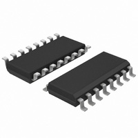
HEF4046BT,653 NXP Semiconductors, HEF4046BT,653 Datasheet - Page 3

HEF4046BT,653
Manufacturer Part Number
HEF4046BT,653
Description
IC PHASE LOCK LOOP W/VCO 16SOIC
Manufacturer
NXP Semiconductors
Type
Phase Lock Loop (PLL)r
Series
HE4000Br
Specifications of HEF4046BT,653
Number Of Circuits
1
Package / Case
16-SOIC (3.9mm Width)
Pll
Yes
Input
Clock
Output
Clock
Ratio - Input:output
1:4
Differential - Input:output
No/No
Frequency - Max
2.7MHz
Divider/multiplier
No/No
Voltage - Supply
3 V ~ 15 V
Operating Temperature
-40°C ~ 85°C
Mounting Type
Surface Mount
Frequency-max
2.7MHz
Supply Voltage (max)
15 V
Supply Voltage (min)
3 V
Maximum Operating Temperature
+ 85 C
Minimum Operating Temperature
- 40 C
Mounting Style
SMD/SMT
Operating Supply Voltage
3.3 V, 5 V, 9 V, 12 V
Lead Free Status / RoHS Status
Lead free / RoHS Compliant
Lead Free Status / RoHS Status
Lead free / RoHS Compliant, Lead free / RoHS Compliant
Other names
933372900653
HEF4046BTD-T
HEF4046BTD-T
HEF4046BTD-T
HEF4046BTD-T
Available stocks
Company
Part Number
Manufacturer
Quantity
Price
Company:
Part Number:
HEF4046BT,653
Manufacturer:
NXP Semiconductors
Quantity:
2 400
Part Number:
HEF4046BT,653
Manufacturer:
NXP/恩智浦
Quantity:
20 000
Philips Semiconductors
FUNCTIONAL DESCRIPTION
VCO part
The VCO requires one external capacitor (C1) and one or
two external resistors (R1 or R1 and R2). Resistor R1 and
capacitor C1 determine the frequency range of the VCO.
Resistor R2 enables the VCO to have a frequency off-set
if required. The high input impedance of the VCO simplifies
the design of low-pass filters; it permits the designer a wide
choice of resistor/capacitor ranges. In order not to load the
low-pass filter, a source-follower output of the VCO input
voltage is provided at pin 10. If this pin (SF
load resistor (R
V
output (pin 4) can either be connected directly to the
comparator input (pin 3) or via a frequency divider. A LOW
level at the inhibit input (pin 5) enables the VCO and the
source follower, while a HIGH level turns off both to
minimize stand-by power consumption.
Phase comparators
The phase-comparator signal input (pin 14) can be
direct-coupled, provided the signal swing is between the
standard HE4000B family input logic levels. The signal
must be capacitively coupled to the self-biasing amplifier
at the signal input in case of smaller swings. Phase
comparator 1 is an EXCLUSIVE-OR network. The signal
and comparator input frequencies must have a 50% duty
January 1995
SS
Phase-locked loop
; if unused, this pin should be left open. The VCO
SF
Fig.2 Pinning diagram.
) should be connected from this pin to
OUT
) is used, a
3
PINNING
1. Phase comparator pulse output
2. Phase comparator 1 output
3. Comparator input
4. VCO output
5. Inhibit input
6. Capacitor C1 connection A
7. Capacitor C1 connection B
8. V
9. VCO input
10. Source-follower output
11. Resistor R1 connection
12. Resistor R2 connection
13. Phase comparator 2 output
14. Signal input
15. Zener diode input for regulated supply.
factor to obtain the maximum lock range. The average
output voltage of the phase comparator is equal to
when there is no signal or noise at the signal input. The
average voltage to the VCO input is supplied by the
low-pass filter connected to the output of phase
comparator 1. This also causes the VCO to oscillate at the
centre frequency (f
defined as the frequency range of input signals on which
the PLL will lock if it was initially out of lock. The frequency
lock range (2 f
signals on which the loop will stay locked if it was initially
in lock. The capture range is smaller or equal to the lock
range.
With phase comparator 1, the range of frequencies over
which the PLL can acquire lock (capture range) depends
on the low-pass filter characteristics and this range can be
made as large as the lock range. Phase comparator 1
enables the PLL system to remain in lock in spite of high
amounts of noise in the input signal. A typical behaviour of
this type of phase comparator is that it may lock onto input
frequencies that are close to harmonics of the VCO centre
frequency. Another typical behaviour is, that the phase
angle between the signal and comparator input varies
between 0 and 180 and is 90 at the centre frequency.
Figure 3 shows the typical phase-to-output response
characteristic.
SS
L
) is defined as the frequency range of input
o
). The frequency capture range (2 f
Product specification
HEF4046B
MSI
1
2
V
c
) is
DD


