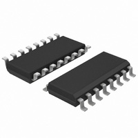
HEF4046BT,653 NXP Semiconductors, HEF4046BT,653 Datasheet - Page 6

HEF4046BT,653
Manufacturer Part Number
HEF4046BT,653
Description
IC PHASE LOCK LOOP W/VCO 16SOIC
Manufacturer
NXP Semiconductors
Type
Phase Lock Loop (PLL)r
Series
HE4000Br
Specifications of HEF4046BT,653
Number Of Circuits
1
Package / Case
16-SOIC (3.9mm Width)
Pll
Yes
Input
Clock
Output
Clock
Ratio - Input:output
1:4
Differential - Input:output
No/No
Frequency - Max
2.7MHz
Divider/multiplier
No/No
Voltage - Supply
3 V ~ 15 V
Operating Temperature
-40°C ~ 85°C
Mounting Type
Surface Mount
Frequency-max
2.7MHz
Supply Voltage (max)
15 V
Supply Voltage (min)
3 V
Maximum Operating Temperature
+ 85 C
Minimum Operating Temperature
- 40 C
Mounting Style
SMD/SMT
Operating Supply Voltage
3.3 V, 5 V, 9 V, 12 V
Lead Free Status / RoHS Status
Lead free / RoHS Compliant
Lead Free Status / RoHS Status
Lead free / RoHS Compliant, Lead free / RoHS Compliant
Other names
933372900653
HEF4046BTD-T
HEF4046BTD-T
HEF4046BTD-T
HEF4046BTD-T
Available stocks
Company
Part Number
Manufacturer
Quantity
Price
Company:
Part Number:
HEF4046BT,653
Manufacturer:
NXP Semiconductors
Quantity:
2 400
Part Number:
HEF4046BT,653
Manufacturer:
NXP/恩智浦
Quantity:
20 000
Philips Semiconductors
Figure 6 shows the state diagram for phase comparator 2.
Each circle represents a state of the comparator. The
number at the top, inside each circle, represents the state
of the comparator, while the logic state of the signal and
comparator inputs are represented by a ‘0’ for a logic LOW
or a ‘1’ for a logic HIGH, and they are shown in the left and
right bottom of each circle.
The transitions from one to another result from either a
logic change at the signal input (S) or the comparator input
(C). A positive-going and a negative-going transition are
shown by an arrow pointing up or down respectively.
January 1995
Phase-locked loop
S : 0 to 1 transition at the signal input.
C
: 1 to 0 transition at the comparator input.
Fig.6 State diagram for comparator 2.
6
The state diagram assumes, that only one transition on
either the signal input or comparator input occurs at any
instant. States 3, 5, 9 and 11 represent the condition at the
output when the p-type driver is ON, while states 2, 4, 10
and 12 determine the condition when the n-type driver is
ON. States 1, 6, 7 and 8 represent the condition when the
output is in its high impedance OFF state; i.e. both p and
n-type drivers are OFF, and the PCP
The condition at output PCP
OUT
for all other states is LOW.
Product specification
OUT
HEF4046B
output is HIGH.
MSI


