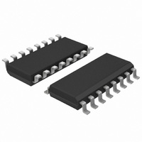
HEF4046BT,653 NXP Semiconductors, HEF4046BT,653 Datasheet - Page 9

HEF4046BT,653
Manufacturer Part Number
HEF4046BT,653
Description
IC PHASE LOCK LOOP W/VCO 16SOIC
Manufacturer
NXP Semiconductors
Type
Phase Lock Loop (PLL)r
Series
HE4000Br
Specifications of HEF4046BT,653
Number Of Circuits
1
Package / Case
16-SOIC (3.9mm Width)
Pll
Yes
Input
Clock
Output
Clock
Ratio - Input:output
1:4
Differential - Input:output
No/No
Frequency - Max
2.7MHz
Divider/multiplier
No/No
Voltage - Supply
3 V ~ 15 V
Operating Temperature
-40°C ~ 85°C
Mounting Type
Surface Mount
Frequency-max
2.7MHz
Supply Voltage (max)
15 V
Supply Voltage (min)
3 V
Maximum Operating Temperature
+ 85 C
Minimum Operating Temperature
- 40 C
Mounting Style
SMD/SMT
Operating Supply Voltage
3.3 V, 5 V, 9 V, 12 V
Lead Free Status / RoHS Status
Lead free / RoHS Compliant
Lead Free Status / RoHS Status
Lead free / RoHS Compliant, Lead free / RoHS Compliant
Other names
933372900653
HEF4046BTD-T
HEF4046BTD-T
HEF4046BTD-T
HEF4046BTD-T
Available stocks
Company
Part Number
Manufacturer
Quantity
Price
Company:
Part Number:
HEF4046BT,653
Manufacturer:
NXP Semiconductors
Quantity:
2 400
Part Number:
HEF4046BT,653
Manufacturer:
NXP/恩智浦
Quantity:
20 000
Philips Semiconductors
DESIGN INFORMATION
VCO component selection
Recommended range for R1 and R2: 10 k to 1 M ; for C1: 50 pF to any practical value.
1. VCO without frequency offset (R2 = ).
2. VCO with frequency offset.
January 1995
No signal on SIGN
Phase angle between
SIGN
Locks on harmonics of
centre frequency
Signal input noise
rejection
Lock frequency
range (2 f
Capture frequency
range (2 f
Centre frequency (f
Phase-locked loop
a) Given f
b) Given f
a) Given f
b) Given f
IN
f
---------- - from the equation
f
---------- - ; use
with Fig.9 to determine R2/R1 to obtain R1.
f
f
CHARACTERISTIC
max
max
min
min
and COMP
L
C
)
)
o
o
max
min
: use f
and f
: calculate f
and f
f
---------- -
f
max
min
IN
IN
o
L
)
o
: calculate f
max
with Fig.7 to determine R1 and C1.
: use f
o
from f
f
---------- -
f
max
min
min
min
with Fig.8 to determine R2 and C1; calculate
=
o
from the equation f
VCO in PLL system adjusts
to centre frequency (f
90 at centre frequency (f
approaching 0 and 180 at
ends of lock range (2 f
yes
high
the frequency range of the input signal on which the loop will stay locked if it was
initially in lock; 2 f
the frequency range of the input signal on which the loop will lock if it was initially
out of lock
depends on low-pass
filter characteristics; f
the frequency of the VCO when VCO
=
f
-------------- - ; use
f
USING PHASE COMPARATOR 1
o
o
1
+
–
2
f
f
f
L
L
max
; use f
f
---------- - with Fig. 9 to determine the ratio R2/R1 to obtain R1.
f
max
min
o
with Fig.7 to determine R1 and C1.
L
min
= full VCO frequency range = f
C
o
= f
9
)
L
)
o
f
o
L
),
f
L
; use f
min
IN
with Fig.8 to determine R2 and C1; calculate
at
VCO in PLL system adjusts to min.
frequency (f
always 0 in lock
(positive-going edges)
no
low
f
C
1
2
USING PHASE COMPARATOR 2
= f
V
DD
L
max
min
)
f
min
Product specification
HEF4046B
MSI


