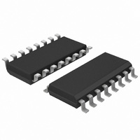
HEF4046BT,653 NXP Semiconductors, HEF4046BT,653 Datasheet - Page 8

HEF4046BT,653
Manufacturer Part Number
HEF4046BT,653
Description
IC PHASE LOCK LOOP W/VCO 16SOIC
Manufacturer
NXP Semiconductors
Type
Phase Lock Loop (PLL)r
Series
HE4000Br
Specifications of HEF4046BT,653
Number Of Circuits
1
Package / Case
16-SOIC (3.9mm Width)
Pll
Yes
Input
Clock
Output
Clock
Ratio - Input:output
1:4
Differential - Input:output
No/No
Frequency - Max
2.7MHz
Divider/multiplier
No/No
Voltage - Supply
3 V ~ 15 V
Operating Temperature
-40°C ~ 85°C
Mounting Type
Surface Mount
Frequency-max
2.7MHz
Supply Voltage (max)
15 V
Supply Voltage (min)
3 V
Maximum Operating Temperature
+ 85 C
Minimum Operating Temperature
- 40 C
Mounting Style
SMD/SMT
Operating Supply Voltage
3.3 V, 5 V, 9 V, 12 V
Lead Free Status / RoHS Status
Lead free / RoHS Compliant
Lead Free Status / RoHS Status
Lead free / RoHS Compliant, Lead free / RoHS Compliant
Other names
933372900653
HEF4046BTD-T
HEF4046BTD-T
HEF4046BTD-T
HEF4046BTD-T
Available stocks
Company
Part Number
Manufacturer
Quantity
Price
Company:
Part Number:
HEF4046BT,653
Manufacturer:
NXP Semiconductors
Quantity:
2 400
Part Number:
HEF4046BT,653
Manufacturer:
NXP/恩智浦
Quantity:
20 000
Philips Semiconductors
Notes
1. Over the recommended component range.
January 1995
VCO
Operating supply
Power dissipation
Maximum operating
Temperature/
Linearity
Duty factor at
Input resistance at
Source follower
Offset voltage
Linearity
Zener diode
Zener voltage
Dynamic resistance
Phase-locked loop
voltage
frequency
frequency
stability
VCO
VCO
VCO
SF
OUT
OUT
IN
IN
minus
V
V
DD
10 P
15
10 f
15
10
15
10
15
10
15
10
15
10 R
15
10
15
10
15
10
15
5
5
5
5
5
5
5
5
5
5
V
V
R
SYMBOL MIN.
max
DD
Z
IN
Z
3
5
0,5
1,0
1,3
0,22 0,30
0,04 0,05
0,01 0,05
8
TYP.
2500
9000
0 0,22
0 0,04
0 0,01
0,50
0,25
0,25
150
10
10
10
1,7
2,0
2,1
1,5
1,7
1,8
0,3
1,0
1,3
7,3
25
1,0
2,0
2,7
50
50
50
6
6
6
MAX.
15
15
%/ C
%
V
V
MHz
MHz
MHz
%/ C
%/ C
%/ C
%/ C
%/ C
%
%
%
%
%
M
M
M
V
V
V
V
V
V
%
%
%
V
W
W
W
as fixed oscillator only
phase-locked loop operation
f
R2 = ; VCO
see also Figs 10 and 11
VCO
R1 = 10 k ; R2 = ;
C1 = 50 pF
no frequency offset
(f
see also note 1
with frequency offset
(f
see also note 1
R1 > 10 k
R1
R1 = 1 M
R
VCO
R
VCO
R
see Fig.13
I
I
o
Z
Z
min
min
SF
SF
SF
= 10 kHz; R1 = 1 M ;
= 50 A
= 1 mA
= 10 k ;
= 50 k ;
> 50 k ;
= 0);
IN
IN
IN
400 k
0);
at V
at
at
Product specification
1
1
HEF4046B
2
2
DD
V
V
IN
;
DD
DD
at
see Fig.13
and Figs 14
15 and 16
1
2
MSI
V
DD
;


