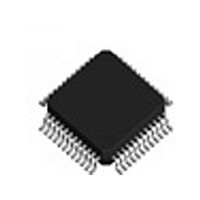
MPC9600AE IDT, Integrated Device Technology Inc, MPC9600AE Datasheet - Page 4

MPC9600AE
Manufacturer Part Number
MPC9600AE
Description
IC PLL CLK DRIVER LV 48-LQFP
Manufacturer
IDT, Integrated Device Technology Inc
Type
PLL Clock Driverr
Datasheet
1.MPC9600AER2.pdf
(14 pages)
Specifications of MPC9600AE
Pll
Yes with Bypass
Input
LVCMOS, LVPECL
Output
LVCMOS
Number Of Circuits
1
Ratio - Input:output
2:22
Differential - Input:output
Yes/No
Frequency - Max
200MHz
Divider/multiplier
Yes/No
Voltage - Supply
2.375 V ~ 3.465 V
Operating Temperature
-40°C ~ 85°C
Mounting Type
Surface Mount
Package / Case
48-LQFP
Frequency-max
200MHz
Number Of Elements
1
Supply Current
5mA
Pll Input Freq (min)
16.67MHz
Pll Input Freq (max)
50MHz
Operating Supply Voltage (typ)
2.5/3.3V
Operating Temp Range
-40C to 85C
Package Type
TQFP
Output Frequency Range
50 to 200MHz
Operating Supply Voltage (min)
2.375V
Operating Supply Voltage (max)
3.465V
Operating Temperature Classification
Industrial
Pin Count
48
Lead Free Status / RoHS Status
Lead free / RoHS Compliant
Available stocks
Company
Part Number
Manufacturer
Quantity
Price
Company:
Part Number:
MPC9600AE
Manufacturer:
IDT, Integrated Device Technology Inc
Quantity:
10 000
Company:
Part Number:
MPC9600AER2
Manufacturer:
IDT
Quantity:
1 186
Company:
Part Number:
MPC9600AER2
Manufacturer:
Sigmatel
Quantity:
77
Company:
Part Number:
MPC9600AER2
Manufacturer:
IDT, Integrated Device Technology Inc
Quantity:
10 000
Part Number:
MPC9600AER2
Manufacturer:
FESSCALE
Quantity:
20 000
IDT™ / ICS™ 2.5V AND 3.3V LVCMOS PLL CLOCK DRIVER
MPC9600
LOW VOLTAGE, 2.5V AND 3.3V LVCMOS PLL CLOCK DRIVER
Table 2. Function Table (Controls)
Table 3. Absolute Maximum Ratings
Table 4. General Specifications
1. V
1. Absolute maximum continuous ratings are those values beyond which damage to the device may occur. Exposure to these conditions or
Symbol
CDM
HBM
C
V
MM
conditions beyond those indicated may adversely affect device reliability. Functional operation under absolute-maximum-rated conditions is
not implied.
C
Symbol
LU
PD
TT
CCA
V
IN
T
I
V
V
OUT
OUT
I
Stor
CC
IN
IN
Control Pin
REF_SEL
FSEL_FB
= GND, PLL off and bypassed for static test and diagnosis.
FSELA
FSELB
FSELC
V
OE
Output Termination Voltage
ESD Protection (Machine Model)
ESD Protection (Human Body Model)
ESD Protection (Charged Device Model)
Latch-Up Immunity
Power Dissipation Capacitance
Input Capacitance
CCA
Supply Voltage
DC Input Voltage
DC Output Voltage
DC Input Current
DC Output Current
Storage Temperature Range
Characteristics
(1)
Feedback Output at VCO/8
Parameter
Output Bank A at VCO/2
Output Bank B at VCO/2
Output Bank C at VCO/2
Outputs Enabled
PLL Bypass
CCLK
0
(1)
4
4000
1500
Min
400
200
V
CC
Typ
4.0
10
–0.3
–0.3
–0.3
Min
–65
÷ 2
Outputs Disabled (except QFB)
Feedback Output at VCO/12
Output Bank C at VCO/4
Output Bank A at VCO/4
Output Bank B at VCO/4
MPC9600 REV. 5 NOVEMBER 10, 2008
Max
PLL Power
PCLK
1
V
V
CC
CC
Unit
Max
±20
±50
125
mA
4.6
pF
pF
V
V
V
V
+ 0.3
+ 0.3
Per output
Inputs
Condition
Unit
mA
mA
°C
V
V
V


