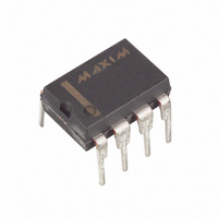
DS1073M-100 Maxim Integrated Products, DS1073M-100 Datasheet

DS1073M-100
Specifications of DS1073M-100
Related parts for DS1073M-100
DS1073M-100 Summary of contents
Page 1
... EconOscillator/Divider PIN ASSIGNMENT OUT0 GND 4 5 DS1073Z-XXX 150-mil SOIC DS1073M-XXX 300-mil DIP XXX = Frequency option FREQUENCY OPTIONS Part No. DS1073M/Z-100 DS1073M/Z-80 DS1073M/Z-66 DS1073M/Z- 70C) or industrial ( DS1073 OSCIN XTAL OE PDN/SELX Max O/P Freq. 100.000MHz 80.000MHz 66.667MHz 60.000MHz = -40C 090503 ...
Page 2
The DS1073 is available in 8-pin DIP or SOIC packages, allowing the generation of a clock signal easily, economically and using minimal board area. BLOCK DIAGRAM Figure 1 PART INTOSC NO. FREQUENCY SUFFIX -100 100.000 MHz -80 80.000 MHz -66 ...
Page 3
PIN DESCRIPTIONS IN/OUT Pin (I/O): This pin is the main oscillator output, with a frequency determined by clock reference, M and N dividers. Except in programming mode this pin is always an output. In programming mode this pin is an ...
Page 4
USER-PROGRAMMABLE REGISTERS The following registers can be programmed by the user to determine operating frequency and mode of operation. Details of how these registers are programmed can be found in a later section, in this section the function of the ...
Page 5
Table 2 DIV1 E/ I MSEL BIT BIT* BIT *Assuming PDN bit = 1, otherwise internal/external selection will be controlled by the DIV WORD ...
Page 6
OPERATION OF OUTPUT ENABLE Since the output enable, internal master oscillator and/or external master oscillator are likely all asynchronous there is the possibility of timing difficulties in the application. difficulties the DS1073 features an “enabling sequencer” to produce predictable results ...
Page 7
Figure 6 SELECT TIMING If the PDN bit is set to 0, the externalor crystal reference. The “Enabling Sequencer” is again employed to ensure this transition occurs in a glitch-free fashion. Two asynchronous clock signals are involved, INTCLK is the ...
Page 8
FROM EXTERNAL TO INTERNAL CLOCK This is accomplished by a low to high transition on the triggered, to allow for the possibility of a clock signal not being present at OSCIN. Note therefore, that if a constant high-level signal is ...
Page 9
POWER-UP When is taken to a high level the following power-up sequence occurs: PDN 1. Enable internal oscillator and/or OSCIN buffer. 2. Set M and N to maximum values. 3. Wait approximately 256 cycles of MCLK for it to stabilize. ...
Page 10
Figure 10 PROGRAMMING Normally when power is applied to the supply voltage pin the device will enter its normal operating mode following the power-on reset sequence. However the device can be made to enter a programming mode if a pullup ...
Page 11
NOTE: To ensure normal operation any external pullup applied to I/O must be greater than 20kW in value. This will cause the I/O pin to remain below STAB Figure 12 TRANSACTION SEQUENCE The sequence for accessing the ...
Page 12
Read DIV Register [A1H] This command allows the bus master to read the DS1073’s DIV register. Write MUX Register [02H] This command allows the bus master to write to the DS1073’s MUX register. Read MUX Register [A2H] This command allows ...
Page 13
READ DATA TIME SLOT Figure 16 RETURN TO NORMAL OPERATION When programming is complete the DS1073 should be powered down. If the pullup resistor on the I/O pin is removed, normal device operation will be restored next time power is ...
Page 14
ABSOLUTE MAXIMUM RATINGS* Voltage on Any Pin Relative to Ground Operating Temperature Storage Temperature Soldering Temperature * This is a stress rating only and functional operation of the device at these or any other conditions above those indicated in the ...
Page 15
AC ELECTRICAL CHARACTERISTICS (T PARAMETER Output Frequency Accuracy Combined Frequency Variation Long Term Stability Maximum Input Frequency Minimum Output Frequency Power-Up Time Enable OUT from PDN ↑ Enable OUT0 from PDN ↑ I/O Hi-Z from PDN ↓ OUT0 Hi-Z from ...
Page 16
AC ELECTRICAL CHARACTERISTICS – CALCULATED PARAMETERS The following characteristics are derived from various device-operating parameters (frequency, mode, etc.). They are not specifically tested or guaranteed and may differ from the min and max limits shown by a small amount due ...
Page 17
DC ELECTRICAL CHARACTERISTICS PARAMETER Supply Voltage High-level Output Voltage (I/O, OUT0) Low-level Output Voltage (I/O, OUT0) High-level Input Voltage Low-level Input Voltage High-level Input Current ( , OE) PDN / SELX (OSCIN) Low-level Input Current( , OE) PDN / SELX ...
Page 18
AC ELECTRICAL CHARACTERISTICS PARAMETER Output Frequency Accuracy Combined Frequency Variation Long Term Stability Maximum Input Frequency Minimum Output Frequency Power-Up Time Enable OUT from PDN ↑ Enable OUT0 from PDN ↑ I/O Hi-Z from PDN ↓ OUT0 Hi-Z from PDN ...


