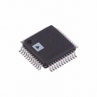
AD9975BST Analog Devices Inc, AD9975BST Datasheet - Page 12

AD9975BST
Manufacturer Part Number
AD9975BST
Description
IC FRONT-END MIXED-SGNL 48-LQFP
Manufacturer
Analog Devices Inc
Series
TxDAC+®r
Datasheet
1.AD9975BST.pdf
(20 pages)
Specifications of AD9975BST
Rohs Status
RoHS non-compliant
Number Of Bits
10
Number Of Channels
1
Voltage - Supply, Analog
3.3V
Voltage - Supply, Digital
3.3V
Package / Case
48-LQFP
Power (watts)
-
Available stocks
Company
Part Number
Manufacturer
Quantity
Price
Company:
Part Number:
AD9975BST
Manufacturer:
ADI
Quantity:
364
AD9975
TRANSMIT PATH
The AD9975 transmit path consists of a digital interface port,
a bypassable 2× interpolation filter, and a transmit DAC. The
clock signals required by these blocks are generated by the inter-
nal PLL. The block diagram below shows the interconnection
between the major functional components of the transmit path.
INTERPOLATION FILTER
The interpolation filter can be programmed to run at a 2×
upsampling ratio in either a low-pass filter or band-pass filter
mode. The transfer functions of these two modes are shown in
TPC 1 and TPC 2, respectively. The y-axes of the figures show
the magnitude response of the filters in dB, and the x-axes show
the frequency normalized to F
the discrete time transfer function of the interpolation filter. The
bottom trace shows the TX path transfer function including the
sin(x)/x transfer function of the DAC. In addition to the two
upsampling modes, the interpolation filter can be programmed
into a pass-through mode if no interpolation filtering is desired.
The table below shows the following parameters as a function of
the mode in which it is programmed.
Latency – The number of clock cycles from the time a digital
impulse is written to the DAC until the peak value is output at
the TX+ and TX– Pins.
Flush – The number of clock cycles from the time a digital
impulse is written to the DAC until the output at the TX+ and
TX– Pins settles to zero.
F
less than the stated magnitude (i.e., 0.1 dB or 1.0 dB).
F
is greater than the stated magnitude (i.e., 40 dB or 50 dB).
Register 7[7:4]
Mode
Latency, F
Flush, F
F
F
F
F
DPLL-A CLOCK DISTRIBUTION
Figure 1 shows the clock signals used in the transmit path. The
DAC sampling clock, f
frequency equal to L × f
value and f
PASS
STOP
PASS
PASS
STOP
STOP
, 0.1 dB
, 1.0 dB
, 40 dB
, 50 dB
– The frequency band over which the pass-band ripple is
– The frequency band over which the stop-band attenuation
DAC
OSCIN
DAC
Table I. Interpolation Filters vs. Mode
Clock Cycles
Clock Cycles
is the frequency of the input to PLL-A. The value
DAC
OSCIN
, is generated by DPLL-A. f
, where L is the PLL clock multiplier
DAC
0x1
2× LPF
30
48
<0.204
<0.207
<0.296
<0.302
. The top trace of the plot shows
0x5
2× BPF, Adj. Image
30
48
>0.296, <0.704
>0.293, <0.707
>0.204, <0.796
<0.198, >0.802
DAC
has a
–12–
of L is programmed through the serial interface port and can be
set to 1, 2, 4, or 8. The transmit path expects a new input sample
at the ADIO interface at a rate of f
filter is being used. If the interpolation filter is bypassed, the
transmit path expects a new input sample at the ADIO interface
at a rate of f
D/A CONVERTER
The AD9975 DAC provides differential output current on the
TX+ and TX– pins. The values of the output currents are comple-
mentary, meaning they will always sum to I
current of the DAC. For example, when the current from TX+
is at full scale, the current from TX– is zero. The two currents
will typically drive a resistive load that will convert the output
currents to a voltage. The TX+ and TX– output currents are
inherently ground seeking and should each be connected to
matching resistors, R
The full-scale output current of the DAC is set by the value of
the resistor placed from the FS ADJ pin to AGND. The rela-
tionship between the resistor, R
current is governed by the following equation:
The full-scale current can be set from 2 to 20 mA. Generally, there
is a trade-off between DAC performance and power consumption.
The best DAC performance will be realized at an I
However, the value of I
consumption of the device.
The single-ended voltage outputs appearing at the TX+ and
TX– nodes are:
Note that the full-scale voltage of V
exceed the maximum output compliance range of 1.5 V to pre-
vent signal compression. To maintain optimum distortion and
linearity performance, the maximum voltages at V
should not exceed ± 0.5 V.
The single-ended full-scale voltage at either output node will be:
The differential voltage, V
and
It should be noted that the differential output impedance of the
DAC is 2 × R
resistors will load down the output voltage accordingly.
DAC.
L
and any load connected across the two output
V
DIFF
L
V
, that are tied directly to AGND.
V
FS
V
DIFF FS
I
V
FS
TX
TX
DIFF
=
adds directly to the overall current
FS
(
+
–
= 39 4 . /
_
I
, appearing across V
=
=
TX
=
I
I
I
+
SET
=
TX
TX
FS
–
I
+
–
DAC
, and the full-scale output
FS
×
I
TX+
×
TX
R
×
R
×
SET
R
/2 if the interpolation
R
–
L
L
and V
R
L
)
×
L
R
FS
L
, the full-scale
TX–
TX+
should not
TX+
FS
and V
of 20 mA.
and V
REV. 0
TX–
TX–
is:


