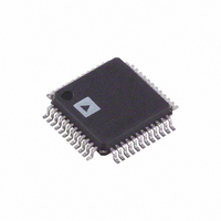
AD9975BST Analog Devices Inc, AD9975BST Datasheet - Page 16

AD9975BST
Manufacturer Part Number
AD9975BST
Description
IC FRONT-END MIXED-SGNL 48-LQFP
Manufacturer
Analog Devices Inc
Series
TxDAC+®r
Datasheet
1.AD9975BST.pdf
(20 pages)
Specifications of AD9975BST
Rohs Status
RoHS non-compliant
Number Of Bits
10
Number Of Channels
1
Voltage - Supply, Analog
3.3V
Voltage - Supply, Digital
3.3V
Package / Case
48-LQFP
Power (watts)
-
Available stocks
Company
Part Number
Manufacturer
Quantity
Price
Company:
Part Number:
AD9975BST
Manufacturer:
ADI
Quantity:
364
AD9975
MSB/LSB Transfers
The AD9975 serial port can support both most significant bit
(MSB) first or least significant bit (LSB) first data formats. The
bit order is controlled by the SPI LSB First Bit (Register 0, Bit 6).
The default value is 0, MSB first. Multibyte data transfers in
MSB format can be completed by writing an instruction byte
that includes the register address of the last address to be accessed.
The AD9975 will automatically decrement the address for each
successive byte required for the multibyte communication cycle.
When the SPI LSB First Bit (Register 0, Bit 6) is set high, the
serial port interprets both instruction and data bytes LSB first.
Multibyte data transfers in LSB format can be completed by
writing an instruction byte that includes the register address of
the first address to be accessed. The AD9975 will automatically
increment the address for each successive byte required for the
multibyte communication cycle.
Address
(hex)
00
01
02
03
04
05
06
07
08
0F
SDATA
SCLK
Figure 6. Timing Diagram Register Read from AD9975
Bit 7
Select 4-Wire LSB/MSB
SPORT
RX LPF
Tuning
Update
Disable
RX LPF Filter Tuning Target [7:0]
RXBOOST
Active Low
CLK-B Equal CLK-A
to OSC IN/4 Equal
INSTRUCTION BIT n
TX Interpolation Filter Select
Bit 6
First
ADC Clock
Source
OSC IN/2
RX LPF
Tuning
Update in
Progress
RXBOOST PGA Gain
to OSC IN Disable
INSTRUCTION BIT n–1
t
DV
Bit 5
Software
Reset
Power-
Down
PLL-A
RX Path
DC Offset HPF
Correction Bypass
Setting
through
Register
CLK-B
Output
Bit 4
Power-
Down
DAC
RX Digital Fast ADC
CLK-A
Output
Disable
Table V. Register Layout
Bit 3
Power-Down Power-Down Power-
Interpolators RX Reference Down ADC Receive Filter
Sampling
Three-State
RX Port
–16–
Figures 7a and 7b show how the serial port words are built for
each of these modes.
Notes on Serial Port Operation
The serial port is disabled and all registers are set to their default
values during a hardware reset. During a software reset, all regis-
ters except Register 0 are set to their default values. Register 0
will remain at the last value sent, with the exception that the
Software Reset Bit will be set to 0.
SENABLE
SENABLE
Figure 7a. Serial Register Interface Timing MSB First
Figure 7b. Serial Register Interface Timing LSB First
SDATA
SDATA
SCLK
SCLK
LPF
RX PGA Gain [4:0]
Bit 2
Wideband RX Enable
R/W I6 (n) I5 (n)
I0
I1
INSTRUCTION CYCLE
INSTRUCTION CYCLE
I2
Version [3:0]
I4
I3
and SPGA and CPGA
Multiplier [1:0]
RX LPF
ADC Output RX Data
on Falling
Bit 1
PLL-A (xL)
1-Pole
Sample TX TX Data
on Falling
TXCLKIN Complement
RXCLK
I3
I4
I5 (n) I6 (n)
I2
I1
R/W
I0
D7 n D6 n
D0 0 D1 0 D2 0
Bit 0
Power-Down 00
RX LPF
Bypass
Input Twos
Output Twos
Complement
DATA TRANSFER CYCLE
DATA TRANSFER CYCLE
Default
(hex)
00
00
01
01
80
00
10
00
00
D6 n
D6 n
REV. 0
D7 n
D7 n
Type
R/W
R/W
R/W
R/W
R/W
R/W
R/W
R/W
R/W
R


