CS5529-ASZ Cirrus Logic Inc, CS5529-ASZ Datasheet - Page 13
CS5529-ASZ
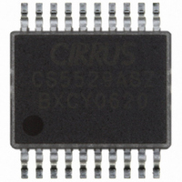
Manufacturer Part Number
CS5529-ASZ
Description
IC ADC 16BIT W/6BIT LATCH 20SSOP
Manufacturer
Cirrus Logic Inc
Datasheet
1.CS5529-ASZ.pdf
(31 pages)
Specifications of CS5529-ASZ
Number Of Converters
1
Package / Case
20-SSOP
Number Of Bits
16
Data Interface
Serial
Power Dissipation (max)
3.5mW
Voltage Supply Source
Analog and Digital, Dual ±
Operating Temperature
-40°C ~ 85°C
Mounting Type
Surface Mount
Number Of Adc Inputs
1
Architecture
Delta-Sigma
Conversion Rate
101 SPs
Resolution
24 bit
Input Type
Voltage
Interface Type
Serial (3-Wire)
Voltage Reference
2.5 V
Maximum Power Dissipation
8 mW
Maximum Operating Temperature
+ 85 C
Mounting Style
SMD/SMT
Minimum Operating Temperature
- 40 C
Lead Free Status / RoHS Status
Lead free / RoHS Compliant
For Use With
598-1015 - EVAL BOARD FOR CS5529
Lead Free Status / Rohs Status
Lead free / RoHS Compliant
Other names
598-1110-5
Available stocks
Company
Part Number
Manufacturer
Quantity
Price
Company:

Part Number:
CS5529-ASZ
Manufacturer:
CIRRUS
Quantity:
88
Part Number:
CS5529-ASZ
Manufacturer:
CIRRUS
Quantity:
20 000
Part Number:
CS5529-ASZR
Manufacturer:
CIRRUS
Quantity:
20 000


Part of the serial port re-initialization sequence (see text for use of command).
End of the serial port re-initialization sequence.
These commands are used to perform a write to or a read from a specific register. The register to be accessed is
selected with the RSB2-RSB0 bits of the command word.
R/W
RSB[4:0]
Serial Port Interface
The CS5529’s serial interface consists of four con-
trol lines: CS, SDI, SDO, and SCLK.
CS, Chip Select, is the control line which enables
access to the serial port. If the CS pin is tied to logic
0, the port can function as a three wire interface.
SDI, Serial Data In, is the data signal used to trans-
fer data to the converters.
SDO, Serial Data Out, is the data signal used to
transfer output data from the converters. The SDO
output will be held at high impedance any time CS
is at logic 1.
SCLK, Serial Clock, is the serial bit-clock which
controls the shifting of data to or from the ADC’s
serial port. The CS pin must be held at logic 0 be-
fore SCLK transitions can be recognized by the
DS246F5
SYNC1
SYNC0
Read/Write Registers
7
1
7
1
7
1
0
1
Register address binary encoded 0 to 31 as follows. All registers are 24 bits long.
Address
000
001
010
011
100
6
1
6
1
6
0
Write Register
Read Register
5
1
5
1
5
0
R/W
Description
Read or Write Offset Register
Read or Write Gain Register
Read or Write Configuration Register
Read Conversion Data Register
Read or Write Offset Gain and Configuration Registers in
this sequence (i.e. one 8-bit command is followed by 72-bits of
data to access the Offset, then the Gain, and then the
Configuration register)
4
1
4
1
4
port logic. To accommodate opto-isolators SCLK
is designed with a Schmitt-trigger input to allow an
opto-isolator with slower rise and fall times to di-
rectly drive the pin. Additionally, SDO is capable
of sinking or sourcing up to 5 mA to directly drive
an opto-isolator LED. SDO will have less than a
400 mV loss in the drive voltage when sinking or
sourcing 5 mA.
Figure 4 illustrates the serial sequence necessary to
write to, or read from the serial port’s registers. A
transfer of data is always initiated by sending the
appropriate 8-bit command (MSB first) to the serial
port (SDI pin). It is important to note that some
commands use information from the configuration
registers to perform the function. For those com-
mands it is important that the correct information is
written to the configuration register first.
RSB2
3
1
3
1
3
RSB1
2
1
2
1
2
RSB0
1
1
1
1
1
CS5529
0
1
0
0
0
0
13
Related parts for CS5529-ASZ
Image
Part Number
Description
Manufacturer
Datasheet
Request
R

Part Number:
Description:
A/D Converter (A-D) IC
Manufacturer:
Cirrus Logic Inc
Datasheet:
Part Number:
Description:
IC Prgrmmbl Dlt Sigma ADC W/6-Bit Latch
Manufacturer:
Cirrus Logic Inc
Datasheet:

Part Number:
Description:
Development Kit
Manufacturer:
Cirrus Logic Inc
Datasheet:
Part Number:
Description:
Development Kit
Manufacturer:
Cirrus Logic Inc
Datasheet:


Part Number:
Description:
High-efficiency PFC + Fluorescent Lamp Driver Reference Design
Manufacturer:
Cirrus Logic Inc
Datasheet:
Part Number:
Description:
Development Kit
Manufacturer:
Cirrus Logic Inc
Datasheet:
Part Number:
Description:
Development Kit
Manufacturer:
Cirrus Logic Inc
Datasheet:

Part Number:
Description:
Development Kit
Manufacturer:
Cirrus Logic Inc
Datasheet:
Part Number:
Description:
Development Kit
Manufacturer:
Cirrus Logic Inc
Datasheet:
Part Number:
Description:
Development Kit
Manufacturer:
Cirrus Logic Inc
Datasheet:
Part Number:
Description:
Development Kit
Manufacturer:
Cirrus Logic Inc
Datasheet:

Part Number:
Description:
Ref Bd For Speakerbar MSA & DSP Products
Manufacturer:
Cirrus Logic Inc