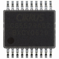
CS5529-ASZ Cirrus Logic Inc, CS5529-ASZ Datasheet - Page 17

CS5529-ASZ
Manufacturer Part Number
CS5529-ASZ
Description
IC ADC 16BIT W/6BIT LATCH 20SSOP
Manufacturer
Cirrus Logic Inc
Datasheet
1.CS5529-ASZ.pdf
(31 pages)
Specifications of CS5529-ASZ
Number Of Converters
1
Package / Case
20-SSOP
Number Of Bits
16
Data Interface
Serial
Power Dissipation (max)
3.5mW
Voltage Supply Source
Analog and Digital, Dual ±
Operating Temperature
-40°C ~ 85°C
Mounting Type
Surface Mount
Number Of Adc Inputs
1
Architecture
Delta-Sigma
Conversion Rate
101 SPs
Resolution
24 bit
Input Type
Voltage
Interface Type
Serial (3-Wire)
Voltage Reference
2.5 V
Maximum Power Dissipation
8 mW
Maximum Operating Temperature
+ 85 C
Mounting Style
SMD/SMT
Minimum Operating Temperature
- 40 C
Lead Free Status / RoHS Status
Lead free / RoHS Compliant
For Use With
598-1015 - EVAL BOARD FOR CS5529
Lead Free Status / Rohs Status
Lead free / RoHS Compliant
Other names
598-1110-5
Available stocks
Company
Part Number
Manufacturer
Quantity
Price
Company:
Part Number:
CS5529-ASZ
Manufacturer:
CIRRUS
Quantity:
88
Part Number:
CS5529-ASZ
Manufacturer:
CIRRUS
Quantity:
20 000
Part Number:
CS5529-ASZR
Manufacturer:
CIRRUS
Quantity:
20 000
Port Flag
The port flag bit in the configuration register allows
the user to select the mode in which conversions
will be presented to the serial port. With the port
flag bit cleared, the user must read the conversion
data register. With the port flag bit set to logic 1, the
user can read the conversion data from the serial
port by first issuing the NULL command to clear
the SDO flag and then issuing 24 SCLKs to read
the conversion word.
Calibration
Calibration is used to set the zero and gain slope of
the ADC’s transfer function. The calibration con-
trol bits in the configuration register allow the user
to perform either self calibration or system calibra-
tion.
The offset and gain calibration steps each take one
conversion cycle to complete. At the end of the cal-
ibration step, the calibration control bits will be set
back to logic 0, and the DF (Done Flag) bit will be
set to a logic 1. For the combination self-calibration
(CC2-CC0= 011; offset calibration followed by
gain calibration), the calibration will take two con-
Offset Register
One LSB represents 2
Offset and data word bits align by MSB (bit MSB-4 of offset register changes bit MSB-4 of data). After reset, all bits
are ‘0’.
DS246F5
23(MSB)
Sign
2
11
0
-13
0
2
2
22
10
0
-14
0
-2
-24
2
2
21
0
9
-15
0
-3
proportion of the input span (bipolar span is 2 times unipolar span).
2
2
20
-16
0
8
0
-4
2
2
19
0
7
-17
0
-5
2
2
18
0
6
-18
0
-6
2
2
17
0
5
-19
0
-7
version cycles to complete and will set the DF bit
after the gain calibration is completed.
Note:
Calibration Registers
The offset calibration result is stored in the offset
register. The result is used during the conversion
process to nullify offset errors. One LSB in the off-
set register is 2
polar span is 2 times the unipolar span). The MSB
in the offset register determines if the offset to be
trimmed is positive or negative (0 positive, 1 nega-
tive). The converter can typically trim ±50 percent
of the input span. Refer to the following Offset
Register and Gain Register descriptions for details.
2
2
16
-20
0
4
0
-8
1) The DF bit will be cleared any time the data
register, the offset register, the gain register,
or the setup register is read. Reading the
configuration register alone will not clear the
DF bit.
2) After the CS5529 is reset, the converter is
functional and can perform measurements
without being calibrated. In this case, the
converter will utilize the initialized values of
the on-chip registers (Gain = 1.0, Offset = 0.0)
to calculate output words. Any initial offset
and gain errors in the internal circuitry of the
chip will remain.
-24
2
2
15
0
3
-21
0
-9
proportion of the input span (bi-
2
2
14
-10
-22
0
2
0
2
2
13
0
1
-23
0
-11
CS5529
2
2
12
-12
0
0
-24
0
17


