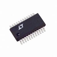
LTC1406IGN#TR Linear Technology, LTC1406IGN#TR Datasheet - Page 11

LTC1406IGN#TR
Manufacturer Part Number
LTC1406IGN#TR
Description
IC ADC 8BIT 20MSPS SAMPLE 24SSOP
Manufacturer
Linear Technology
Datasheet
1.LTC1406IGNPBF.pdf
(16 pages)
Specifications of LTC1406IGN#TR
Number Of Bits
8
Sampling Rate (per Second)
20M
Data Interface
Parallel
Number Of Converters
1
Power Dissipation (max)
225mW
Voltage Supply Source
Analog and Digital, Dual ±
Operating Temperature
-40°C ~ 85°C
Mounting Type
Surface Mount
Package / Case
24-SSOP (0.150", 3.90mm Width)
Lead Free Status / RoHS Status
Contains lead / RoHS non-compliant
Available stocks
Company
Part Number
Manufacturer
Quantity
Price
APPLICATIONS
LT1229/LT1230: Dual and Quad 100MHz Current Feed-
back Amplifiers. 2V to 15V supplies. Low noise. 6mA
supply current each amplifier.
LT1259/LT1260: Dual and Triple 130MHz Current Feed-
back Amplifiers. 2V to 14V supplies. 5mA supply cur-
rent. Low distortion. Low noise.
LT1363: 70MHz Voltage Feedback Amplifier. 2.5V to
LT1364/LT1365: Dual and Quad 70MHz Voltage Feedback
Amplifiers. 2.5V to 15V supplies. 7.5mA supply current
per amplifier. Low distortion.
Input Filtering
The noise and the distortion of the input amplifier and
other circuitry must be considered since they will add to
the LTC1406 noise and distortion. The small-signal band-
width of the sample-and-hold circuit is 250MHz. Any noise
or distortion products that are present at the analog inputs
will be summed over this entire bandwidth. Noisy input
circuitry should be filtered prior to the analog inputs to
minimize noise. A simple 1-pole RC filter is sufficient for
many applications. For example, Figure 9 shows a 220pF
capacitor from A
limit the input bandwidth to 9.6MHz. The 220pF capacitor
also acts as a charge reservoir for the input sample-and-
hold and isolates the ADC input from sampling glitch sen-
sitive circuitry. Larger value capacitors may be substituted
to further limit the input bandwidth. High quality capaci-
tors and resistors should be used since these components
can add distortion. NPO and silver mica type dielectric
capacitors have excellent linearity. Carbon surface mount
15V supplies. 7.5mA supply current. Low distortion.
ANALOG INPUT
1.5V TO 3.5V
IN
Figure 9. RC Input Filter
+
U
to A
220pF
IN
75
2.5V
INFORMATION
U
–
and a 75 source resistor to
A
A
V
W
IN
IN
REF
LTC1406
+
–
1406 F09
U
resistors can also generate distortion from self-heating
and from damage that may occur during soldering. Metal
film surface mount resistors are much less susceptible to
both problems.
Input/Output Characteristics
Figure 10 shows the ideal input/output characteristics for
the LTC1406. The code transitions occur midway between
successive integer LSB values (i.e., – FS + 0.5LSB, – FS +
1.5LSB, – FS + 2.5LSB...FS – 1.5LSB, FS – 0.5LSB). The
output is straight binary with 1LSB = FS – (– FS)/256 = 2V/
256 = 7.8125mV. The OF/UF bit indicates that the input has
exceeded full scale and can be used to detect an overrange
or underrange condition. A logic high output on the OF/UF
pin with an output code of 0000 0000 indicates the input
is less than the negative full scale. A logic high output on
the OF/UF pin with an output code of 1111 1111 indicates
that the input is greater than the positive full scale. A logic
low output on the OF/UF pin indicates the input is within
the full-scale range of the converter.
In applications where absolute accuracy is important, off-
set and full-scale errors can be adjusted to zero. Offset
error must be adjusted before full-scale error. Zero offset
is achieved by adjusting the offset applied to the A
For zero offset error, apply a voltage equal to the input
1111 1111
1111 1110
1111 1101
1000 0001
1000 0000
0111 1111
0111 1110
0000 0010
0000 0001
0000 0000
OF/UF BIT
Figure 10. Transfer Characteristics
–FS
INPUT VOLTAGE (V)
–1
LSB
0
LSB
1
FS – 1LSB
LTC1406
1406 F10
IN
11
–
input.


