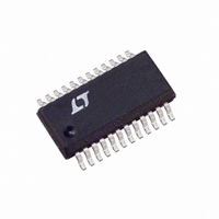
LTC1406IGN#TR Linear Technology, LTC1406IGN#TR Datasheet - Page 6

LTC1406IGN#TR
Manufacturer Part Number
LTC1406IGN#TR
Description
IC ADC 8BIT 20MSPS SAMPLE 24SSOP
Manufacturer
Linear Technology
Datasheet
1.LTC1406IGNPBF.pdf
(16 pages)
Specifications of LTC1406IGN#TR
Number Of Bits
8
Sampling Rate (per Second)
20M
Data Interface
Parallel
Number Of Converters
1
Power Dissipation (max)
225mW
Voltage Supply Source
Analog and Digital, Dual ±
Operating Temperature
-40°C ~ 85°C
Mounting Type
Surface Mount
Package / Case
24-SSOP (0.150", 3.90mm Width)
Lead Free Status / RoHS Status
Contains lead / RoHS non-compliant
Available stocks
Company
Part Number
Manufacturer
Quantity
Price
LTC1406
TI I G DIAGRA
6
PIN
AV
log ground plane with 10 F tantalum in parallel with 0.1 F
or 10 F ceramic.
AGND (Pin 10): Analog Ground. Tie to analog ground plane.
DGND (Pin 11): Digital Ground for Internal Logic. Tie to
analog ground plane.
DV
with 10 F tantalum in parallel with 0.1 F or 10 F ceramic.
NC (Pins 13, 14): No Internal Connection.
AV
PIN
1
2
3
4
5
6
7
8
9
10
11
12
13 to 14
15 to 22
23
24
DD
W
DD
U
DD
= DV
(Pin 12): Digital 5V Positive Supply. Bypass to DGND
(Pin 9): Analog 5V Positive Supply. Bypass to ana-
FUNCTIONS
U
DD
= V
U
NAME
OGND
OV
SHDN
V
V
AGND
A
A
AV
AGND
DGND
DV
NC
D7 to D0
OF/UF
CLK
BIAS
REF
IN
IN
DATA OUT
DD
DD
DD
DD
+
–
ANALOG
SIGNAL
CLOCK
U
DESCRIPTION
Ground for Output Drivers
Supply for Output Drivers
Shutdown Input, Active Low
Internal Bias Voltage
External Reference Input
Analog Ground, Clean Ground
Positive Analog Input, 1V Span
Negative Analog Input
Analog Supply
Analog Ground, Substrate Ground
Digital Ground
Digital Supply
No Connect, No Internal Connection
Data Outputs
Overflow/Underflow Output
Clock Input
N – 1
W
N – 6
N
t
6
N – 5
N + 1
t
3
N – 4
t
2
N + 2
D7 to D0 (Pins 15 to 22): Digital Data Outputs. The out-
puts swing between OV
OF/UF (Pin 23): Overflow/Underflow Bit. OF/UF high with
D7 to D0 all high indicates an overrange, OF/UF high with
D7 to D0 all low indicates an underrange condition. OF/UF
low indicates a conversion within the normal input range.
The outputs swing between OV
CLK (Pin 24): Clock Input. Internal sample-and-hold tracks
the input signal when CLK is high and samples the input
signal on the falling edge.
N – 3
t
OGND
OGND
5
4.75
4.75
MIN
2.7
1.9
0
2
0
0
0
N + 3
t
1
NOMINAL (V)
N – 2
3 or 5
TYP
2.2
2.5
0
0
5
0
0
5
N + 4
N – 1
OV
OV
MAX
5.25
DD
5.25
5.25
V
V
V
V
2.5
3
DD
DD
DD
DD
DD
DD
N + 5
and OGND.
t
4
DD
ABSOLUTE MAXIMUM (V)
N
and OGND.
N + 6
– 0.3
– 0.3
– 0.3
– 0.3
– 0.3
– 0.3
– 0.3
– 0.3
– 0.3
– 0.3
– 0.3
– 0.3
– 0.3
– 0.3
– 0.3
MIN
1406 TD
V
V
V
V
V
V
V
V
V
V
DD
DD
DD
DD
DD
DD
DD
DD
DD
DD
MAX
10
10
6
6
6
+ 0.3
+ 0.3
+ 0.3
+ 0.3
+ 0.3
+ 0.3
+ 0.3
+ 0.3
+ 0.3
+ 0.3


