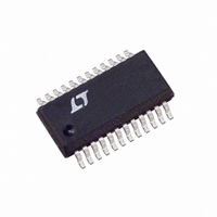
LTC1406IGN#TR Linear Technology, LTC1406IGN#TR Datasheet - Page 2

LTC1406IGN#TR
Manufacturer Part Number
LTC1406IGN#TR
Description
IC ADC 8BIT 20MSPS SAMPLE 24SSOP
Manufacturer
Linear Technology
Datasheet
1.LTC1406IGNPBF.pdf
(16 pages)
Specifications of LTC1406IGN#TR
Number Of Bits
8
Sampling Rate (per Second)
20M
Data Interface
Parallel
Number Of Converters
1
Power Dissipation (max)
225mW
Voltage Supply Source
Analog and Digital, Dual ±
Operating Temperature
-40°C ~ 85°C
Mounting Type
Surface Mount
Package / Case
24-SSOP (0.150", 3.90mm Width)
Lead Free Status / RoHS Status
Contains lead / RoHS non-compliant
Available stocks
Company
Part Number
Manufacturer
Quantity
Price
ABSOLUTE
CO
A
LTC1406
AV
Supply Voltage (V
Analog Input Voltage (Note 3) .... – 0.3V to (V
Digital Input Voltage (Note 4) .................. – 0.3V to 10V
Digital Output Voltage ................. – 0.3V to (V
Power Dissipation.............................................. 500mW
Ambient Operation Temperature Range
Storage Temperature Range ................. – 65 C to 150 C
Lead Temperature (Soldering, 10 sec).................. 300 C
The denotes specifications which apply over the full operating temperature range, otherwise specifications are T
(Notes 5, 6)
The denotes specifications which apply over the full operating temperature range, otherwise specifications are T
2
PARAMETER
Resolution (No Missing Codes)
Integral Linearity Error
Differential Linearity Error
Offset Error
Gain Error
SYMBOL PARAMETER
V
I
C
t
t
CMRR
V
IN
AP
jitter
IN
IN
BIAS
U
DD
LTC1406C................................................ 0 C to 70 C
LTC1406I............................................ – 40 C to 85 C
U
A
= OV
LOG
VERTER
Analog Input Span [(A
Input (A
Analog Input Leakage Current
Analog Input Capacitance
Input Bandwidth
Sample-and-Hold Aperture Delay Time
Sample-and-Hold Aperture Delay Time Jitter
Analog Input Common Mode Rejection Ratio
Internal Bias Voltage
DD
= DV
IN
DD
I
+
U
or A
DD
W
MAXIMUM
= V
PUT
) ................................................. 6V
IN
DD
C
–
) Range
HARA TERISTICS
(Notes 1, 2)
IN
W W
+
) – (A
(Note 5)
IN
C
–
)] (Note 9)
RATINGS
U
CONDITIONS
4.75V V
Voltage On Either A
CLK = 0
CLK = 1
CLK = 0
– 2.5V < (A
No Load
DD
DD
CONDITIONS
(Note 7)
(Note 8)
With External 2.5V Reference
+ 0.3V)
+ 0.3V)
DD
IN
–
= A
5.25V
IN
IN
+
PACKAGE/ORDER
Consult factory for Military grade parts.
) < 2.5V
+
or A
IN
OGND
DGND
SHDN
AGND
AGND
OV
V
AV
DV
V
–
A
A
BIAS
REF
IN
IN
DD
DD
DD
+
–
T
JMAX
24-LEAD PLASTIC SSOP
10
11
12
1
2
3
4
5
6
7
8
9
= 110 C,
GN PACKAGE
TOP VIEW
JA
= 85 C/ W
24
23
22
21
20
19
18
17
16
15
14
13
CLK
OF/UF
D7
D6
D5
D4
D3
D2
D1
D0
NC
NC
MIN
MIN
8
0
INFORMATION
U
TYP
TYP
250
2.2
0.25
60
0.5
4
2
3
5
1
1
1
A
A
ORDER PART
LTC1406CGN
LTC1406IGN
= 25 C.
= 25 C.
W
NUMBER
MAX
MAX
V
DD
1
1
8
5
5
UNITS
UNITS
ps
U
MHz
LSB
LSB
LSB
LSB
RMS
Bits
dB
pF
pF
ns
V
V
A
V


