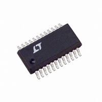
LTC1406IGN#TR Linear Technology, LTC1406IGN#TR Datasheet - Page 7

LTC1406IGN#TR
Manufacturer Part Number
LTC1406IGN#TR
Description
IC ADC 8BIT 20MSPS SAMPLE 24SSOP
Manufacturer
Linear Technology
Datasheet
1.LTC1406IGNPBF.pdf
(16 pages)
Specifications of LTC1406IGN#TR
Number Of Bits
8
Sampling Rate (per Second)
20M
Data Interface
Parallel
Number Of Converters
1
Power Dissipation (max)
225mW
Voltage Supply Source
Analog and Digital, Dual ±
Operating Temperature
-40°C ~ 85°C
Mounting Type
Surface Mount
Package / Case
24-SSOP (0.150", 3.90mm Width)
Lead Free Status / RoHS Status
Contains lead / RoHS non-compliant
Available stocks
Company
Part Number
Manufacturer
Quantity
Price
FUNCTIONAL BLOCK DIAGRA
APPLICATIONS
Conversion Details
The LTC1406 uses an internal sample-and-hold circuit and
a pipeline quantizing architecture to convert an analog
signal to an 8-bit parallel output. With CLK high the input
switches are closed and the analog input will be acquired
on the input sampling capacitors C
On the falling edge of CLK the input switches open, captur-
ing the input signal. The sampling capacitors are then
shorted together and the charge is transferred to the hold
U
A
A
IN
IN
+
–
Figure 1. Input Sample-and-Hold Amplifier
CLK
CLK
U
CLK
U
C
C
S
S
A
A
CLK
IN
IN
CLK
INFORMATION
+
–
U
24
7
8
AV
+
–
DD
CLK
CLK
C
C
9
TRACK-AND-
HOLD AMP
S
H
H
2.5k
W
CIRCUITRY
(see Figure 1).
CLOCK
V
BIAS
4
2.2V
1.95k
1406 F01
AGND
TO NEXT STAGE
10
U
W
SHDN
3
PIPELINE
8-BIT
ADC
DV
V
REF
DD
12
5
capacitors C
output of the track-and-hold amplifier that is proportional
to the input signal. This differential voltage is fed into a
comparator that determines the most significant bit and
subtracts the result. The residue is then amplified by two
and passed to the next stage via a similar sample-and-hold
circuit. This continues down the eight pipeline stages. The
comparator outputs are then combined in a digital error
correction circuit. The 8-bit word is available at the output,
five clock cycles after the sampling edge.
Dynamic Performance
The LTC1406 has excellent wideband sampling capability.
The sample-and-hold amplifier has a small-signal input
bandwidth of 250MHz allowing the ADC to undersample
input signals with frequencies well beyond the converter’s
Nyquist frequency. FFT (Fast Fourier Transform) test tech-
niques are used to test the ADC’s frequency response,
distortion and noise at the rated throughput. By applying
a low distortion sine wave and analyzing the digital output
using an FFT algorithm, the ADC’s spectral content can be
examined for frequencies outside the fundamental. Figure
2 shows a typical LTC1406 FFT plot.
AGND
6
DIGITAL
DGND
DATA
11
H
resulting in a differential DC voltage on the
DRIVERS
OUTPUT
OV
OGND
DD
1
2
23
22
21
20
19
18
17
16
15
1406 BD
OF/UF
D7
D6
D5
D4
D3
D2
D1
D0
LTC1406
7


