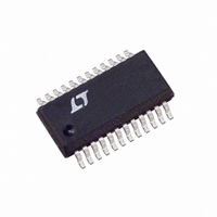
LTC1406IGN#TR Linear Technology, LTC1406IGN#TR Datasheet

LTC1406IGN#TR
Specifications of LTC1406IGN#TR
Available stocks
Related parts for LTC1406IGN#TR
LTC1406IGN#TR Summary of contents
Page 1
... The ADC has an 8-bit parallel output port with separate power supply and ground allowing easy interface to 3V digital systems. The pipelined architecture has five clock cycles of data latency. , LTC and LT are registered trademarks of Linear Technology Corporation. U DGND OV DD ...
Page 2
LTC1406 ABSOLUTE MAXIMUM (Notes Supply Voltage (V ) ................................................. 6V DD Analog Input Voltage (Note 3) .... – 0. Digital Input Voltage ...
Page 3
ACCURACY The denotes specifications which apply over the full operating temperature range, otherwise specifications are T SYMBOL PARAMETER S/( Signal-to-Noise Plus Distortion Ratio THD Total Harmonic Distortion SFDR Spurious Free Dynamic Range IMD ...
Page 4
LTC1406 CHARACTERISTICS The denotes specifications which apply over the full operating temperature range, otherwise specifications are T SYMBOL PARAMETER f Maximum Sampling Frequency SMPL(MAX) t Clock Period 1 t Pulse Width High 2 t Pulse ...
Page 5
W U TYPICAL PERFORMANCE CHARACTERISTICS Spurious-Free Dynamic Range vs Input Frequency 100k 1M 10M 100M INPUT FREQUENCY (Hz) 1406 G04 Integral Nonlinearity vs Output Code 1.0 0.5 0 –0.5 –1.0 128 0 ...
Page 6
LTC1406 PIN FUNCTIONS AV (Pin 9): Analog 5V Positive Supply. Bypass to ana- DD log ground plane with 10 F tantalum in parallel with 0 ceramic. AGND (Pin 10): Analog Ground. Tie to ...
Page 7
U U FUNCTIONAL BLOCK DIAGRA 24 CLK – APPLICATIONS INFORMATION Conversion Details The LTC1406 uses an internal sample-and-hold circuit and a pipeline quantizing architecture to convert an analog signal ...
Page 8
LTC1406 U U APPLICATIONS INFORMATION 0 f SAMPLE – 1.000977MHz IN1 SFDR = 64.8dB –20 SINAD = 48.6dB –30 –40 –50 –60 –70 –80 –90 –100 FREQUENCY (Hz) Figure 2a. Nonaveraged, ...
Page 9
U U APPLICATIONS INFORMATION 0 –10 –20 –30 –40 –50 THD –60 –70 3RD HARMONIC 2ND HARMONIC –80 100k 1M 10M INPUT FREQUENCY (Hz) Figure 4. Distortion vs Input Frequency 0 f SAMPLE – 3.500977MHz IN1 f = ...
Page 10
... The following list is a summary of the op amps that are suitable for driving the LTC1406. More detailed informa- tion is available in the Linear Technology Databooks and ) can vary REF on the LinearView ® ...
Page 11
U U APPLICATIONS INFORMATION LT1229/LT1230: Dual and Quad 100MHz Current Feed- back Amplifiers 15V supplies. Low noise. 6mA supply current each amplifier. LT1259/LT1260: Dual and Triple 130MHz Current Feed- back Amplifiers 14V supplies. 5mA supply cur- ...
Page 12
LTC1406 U U APPLICATIONS INFORMATION common mode voltage minus 3.90625mV (i.e., – 0.5LSB) – and adjust the offset at the A input until the output code IN flickers between 0111 1111 and 1000 0000. For full-scale adjustment, an input voltage ...
Page 13
U U APPLICATIONS INFORMATION shutdown. It may also be desirable to isolate the data out- put pins from the bus to reduce the load capacitance. To resume normal operation the SHDN pin must be brought high and typically 20 clock ...
Page 14
LTC1406 U U APPLICATIONS INFORMATION ...
Page 15
... FLASH SHALL NOT EXCEED 0.010" (0.254mm) PER SIDE Information furnished by Linear Technology Corporation is believed to be accurate and reliable. However, no responsibility is assumed for its use. Linear Technology Corporation makes no represen- tation that the interconnection of its circuits as described herein will not infringe on existing patent rights. ...
Page 16
... LTC1446L 2.7V to 5.5V, Output Swings from GND to REF, REF Input Can Be CC Tied LTC1458 LTC1458L 4.5V to 5.5V 4.095V OUT = 2.7V to 5.5V 2.5V CC OUT = 4.5V to 5.5V 4.095V OUT = 2.7V to 5.5V 2.5V CC OUT 1406f LT/TP 0299 4K • PRINTED IN USA LINEAR TECHNOLOGY CORPORATION 1998 ...


