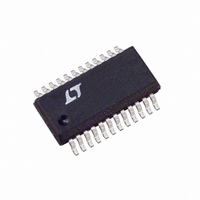
LTC1406IGN#TR Linear Technology, LTC1406IGN#TR Datasheet - Page 9

LTC1406IGN#TR
Manufacturer Part Number
LTC1406IGN#TR
Description
IC ADC 8BIT 20MSPS SAMPLE 24SSOP
Manufacturer
Linear Technology
Datasheet
1.LTC1406IGNPBF.pdf
(16 pages)
Specifications of LTC1406IGN#TR
Number Of Bits
8
Sampling Rate (per Second)
20M
Data Interface
Parallel
Number Of Converters
1
Power Dissipation (max)
225mW
Voltage Supply Source
Analog and Digital, Dual ±
Operating Temperature
-40°C ~ 85°C
Mounting Type
Surface Mount
Package / Case
24-SSOP (0.150", 3.90mm Width)
Lead Free Status / RoHS Status
Contains lead / RoHS non-compliant
Available stocks
Company
Part Number
Manufacturer
Quantity
Price
APPLICATIONS
Figure 6. Spurious-Free Dynamic Range vs
Input Frequency
Figure 4. Distortion vs Input Frequency
–100
–10
–20
–30
–40
–50
–60
–70
–80
Figure 5. Intermodulation Distortion Plot
–10
–20
–30
–40
–50
–60
–70
–80
–90
70
60
50
40
30
20
10
0
100k
0
100k
0
0
2ND HARMONIC
1
U
THD
2
INPUT FREQUENCY (Hz)
INPUT FREQUENCY (Hz)
3
INFORMATION
1M
1M
FREQUENCY (MHz)
U
4
5
f
f
f
SAMPLE
IN1
IN2
3RD HARMONIC
6
= 3.500977MHz
= 3.598633MHz
10M
10M
W
7
= 20MHz
8
1406 G03
1406 G04
1406 G05
9
100M
100M
10
U
If two pure sine waves of frequencies f
to the ADC input, nonlinearities in the ADC transfer func-
tion can create distortion products at the sum and differ-
ence frequencies of mf
etc. For example, the 2nd order IMD terms include (f
If the two input sine waves are equal in magnitude, the
value (in decibels) of the 2nd order IMD products can be
expressed by the following formula:
Peak Harmonic or Spurious Noise
The peak harmonic or spurious noise is the largest spec-
tral component excluding the input signal and DC. This
value is expressed in decibel relative to the RMS value of
a full-scale input signal (see Figure 6).
Input Bandwidth
The input bandwidth is that input frequency at which the
amplitude of the reconstructed fundamental is reduced by
3dB for a full-scale input signal. The LTC1406 has been
designed for wide input bandwidth (250MHz), allowing
the ADC to undersample input signals with frequencies
above the converter’s Nyquist frequency. The noise floor
stays very low at high frequencies; S/(N + D) becomes
dominated by distortion at frequencies far beyond Nyquist.
Analog Inputs
The LTC1406 has a unique differential sample-and-hold
circuit that allows rail-to-rail inputs. The A
inputs are sampled at the same time and the ADC will
always convert the difference of [(A
dent of the common mode voltage. Any unwanted signal
that is common to both inputs will be rejected by the com-
mon mode rejection of the sample-and-hold circuit. The
common mode rejection holds up to extremely high fre-
quencies (see Figure 7).
The inputs can be driven differentially or single-ended. In
differential mode, both inputs are driven 0.5V out of
phase with each other. In single-ended mode, the nega-
tive input is tied to a fixed voltage and A
IMD f
a
f
b
20 log
a
Amplitude at f
nf
b
Amplitude at
, where m and n = 0, 1, 2, 3,
IN
+
) – (A
a
and f
IN
a
LTC1406
+
f
a
IN
is used as the
IN
b
f
–
b
)] indepen-
are applied
+
and A
a
9
f
IN
b
).
–


