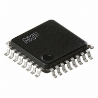
ADC1002S020HL/C1,1 NXP Semiconductors, ADC1002S020HL/C1,1 Datasheet - Page 7

ADC1002S020HL/C1,1
Manufacturer Part Number
ADC1002S020HL/C1,1
Description
IC ADC 10BIT PAR 20MHZ 32-LQFP
Manufacturer
NXP Semiconductors
Datasheet
1.ADC1002S020HLC11.pdf
(19 pages)
Specifications of ADC1002S020HL/C1,1
Number Of Bits
10
Sampling Rate (per Second)
20M
Data Interface
Parallel
Number Of Converters
1
Power Dissipation (max)
73mW
Voltage Supply Source
Analog and Digital
Operating Temperature
-40°C ~ 85°C
Mounting Type
Surface Mount
Package / Case
32-LQFP
Lead Free Status / RoHS Status
Lead free / RoHS Compliant
Other names
935286648118
ADC1002S020HL/C1-T
ADC1002S020HL/C1-T
ADC1002S020HL/C1-T
ADC1002S020HL/C1-T
Available stocks
Company
Part Number
Manufacturer
Quantity
Price
Company:
Part Number:
ADC1002S020HL/C1,1
Manufacturer:
IDT, Integrated Device Technology Inc
Quantity:
10 000
NXP Semiconductors
Table 6.
V
together; V
specified.
ADC1002S020_2
Product data sheet
Symbol
V
I
R
TC
V
V
Digital outputs D9 to D0 and IR (Referenced to V
V
V
I
Switching characteristics; Clock input CLK; see
f
t
t
Analog signal processing (f
Linearity
INL
DNL
Input set response; see
t
t
Harmonics; see
THD
Signal-to-Noise ratio; see
S/N
Effective bits; see
ENOB
ref
OZ
clk(max)
w(clk)H
w(clk)L
s(LH)
s(HL)
DDA
ref(dif)
offset
i(p-p)
OL
OH
lad
Rlad
= V7 to V9 = 3.3 V; V
i(p-p)
Characteristics
Parameter
differential reference
voltage
reference current
ladder resistance
ladder resistor
temperature coefficient
offset voltage
peak-to-peak input
voltage
LOW-level output
voltage
HIGH-level output
voltage
OFF-state output current 0.5 V < V
maximum clock
frequency
HIGH clock pulse width
LOW clock pulse width
integral non-linearity
differential non-linearity
LOW to HIGH settling
time
HIGH to LOW settling
time
total harmonic distortion f
signal-to-noise ratio
effective number of bits
= 1.83 V; C
Figure 9
Figure 9
Figure 8
[5]
Figure 9
DDD
L
[5]
= 20 pF; T
…continued
clk
= V4 to V3 = V18 to V19 = 3.3 V; V
[4]
= 20 MHz)
[5]
amb
Conditions
V
BOTTOM
TOP
I
I
ramp input; see
ramp input; see
full-scale square wave
full-scale square wave
without harmonics;
f
O
O
i
i
f
f
f
i
i
i
RT
= 1 MHz
= 1 MHz
= 0 C to 70 C; typical values measured at T
= 300 KHz
= 1 MHz
= 3.58 MHz
= 1 mA
= 1 mA
V
RB
Rev. 02 — 13 August 2008
O
< V
SSD
Figure
DDO
)
Figure 6
Figure 7
4;
[1]
DDO
[2]
[2]
[3]
= V20 to V21 = 3.3 V; V
Min
1.9
-
-
-
-
-
-
1.66
0
V
20
15
15
-
-
-
-
-
-
-
-
-
20
DDO
0.5
Single 10 bits ADC, up to 20 MHz
Typ
2.1
7.2
290
539
1860
135
135
1.83
-
-
-
-
-
-
4
4
60
9.5
9.3
8.0
amb
1
0.25
63
ADC1002S020
= 25 C unless otherwise
SSA
, V
SSD
Max
3.0
-
-
-
-
-
-
2.35
0.5
V
+20
-
-
-
6
6
-
-
-
2
0.7
CCO
© NXP B.V. 2008. All rights reserved.
and V
SSO
shorted
Unit
V
mA
m /K
ppm
mV
mV
V
V
V
MHz
ns
ns
LSB
LSB
ns
ns
dB
dB
bits
bits
bits
A
7 of 19


