PIC18F65K90-I/MR Microchip Technology, PIC18F65K90-I/MR Datasheet - Page 119
PIC18F65K90-I/MR
Manufacturer Part Number
PIC18F65K90-I/MR
Description
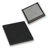
32kB Flash, 2kB RAM, 1kB EE, NanoWatt XLP, LCD 64 QFN 9x9x0.9mm TUBE
Manufacturer
Microchip Technology
Series
PIC® XLP™ 18Fr
Datasheet
1.PIC18F65K90-IMR.pdf
(570 pages)
Specifications of PIC18F65K90-I/MR
Processor Series
PIC18F
Core
PIC
Data Bus Width
8 bit
Program Memory Type
Flash
Program Memory Size
32 KB
Data Ram Size
2 KB
Interface Type
I2C, SPI
Maximum Clock Frequency
64 MHz
Number Of Timers
8
Operating Supply Voltage
1.8 V to 5.5 V
Maximum Operating Temperature
+ 125 C
3rd Party Development Tools
52715-96, 52716-328, 52717-734, 52712-325, EWPIC18
Minimum Operating Temperature
- 40 C
On-chip Adc
12 bit, 16 Channel
Core Processor
PIC
Core Size
8-Bit
Speed
64MHz
Connectivity
I²C, LIN, SPI, UART/USART
Peripherals
Brown-out Detect/Reset, LCD, POR, PWM, WDT
Number Of I /o
53
Eeprom Size
1K x 8
Ram Size
2K x 8
Voltage - Supply (vcc/vdd)
1.8 V ~ 5.5 V
Data Converters
A/D 16x12b
Oscillator Type
Internal
Operating Temperature
-40°C ~ 85°C
Package / Case
64-VFQFN Exposed Pad
Lead Free Status / Rohs Status
Details


EXAMPLE 7-3:
7.5.2
Depending on the application, good programming
practice may dictate that the value written to the
memory should be verified against the original value.
This should be used in applications where excessive
writes can stress bits near the specification limit.
7.5.3
If a write is terminated by an unplanned event, such as
loss of power or an unexpected Reset, the memory
location just programmed should be verified and repro-
grammed if needed. If the write operation is interrupted
by a MCLR Reset or a WDT Time-out Reset during
normal operation, the user can check the WRERR bit
and rewrite the location(s) as needed.
TABLE 7-2:
2009-2011 Microchip Technology Inc.
TBLPTRU
TBPLTRH Program Memory Table Pointer High Byte (TBLPTR<15:8>)
TBLPTRL Program Memory Table Pointer Low Byte (TBLPTR<7:0>)
TABLAT
INTCON
EECON2
EECON1
IPR6
PIR6
PIE6
Legend: — = unimplemented, read as ‘0’. Shaded cells are not used during Flash/EEPROM access.
Note 1:
PROGRAM_MEMORY
Name
Required
Sequence
Bit 21 of TBLPTRU allows access to the device Configuration bits.
WRITE VERIFY
UNEXPECTED TERMINATION OF
WRITE OPERATION
Program Memory Table Latch
EEPROM Control Register 2 (not a physical register)
GIE/GIEH PEIE/GIEL TMR0IE
EEPGD
Bit 7
—
—
—
—
REGISTERS ASSOCIATED WITH PROGRAM FLASH MEMORY
BSF
BCF
BSF
BCF
MOVLW
MOVWF
MOVLW
MOVWF
BSF
BSF
BCF
WRITING TO FLASH PROGRAM MEMORY (CONTINUED)
CFGS
Bit 6
EECON1, EEPGD
EECON1, CFGS
EECON1, WREN
INTCON, GIE
0x55
EECON2
0xAA
EECON2
EECON1, WR
INTCON, GIE
EECON1, WREN
—
—
—
—
bit 21
Bit 5
—
—
—
—
(1)
Program Memory Table Pointer Upper Byte (TBLPTR<20:16>)
INT0IE
FREE
EEIP
EEIF
EEIE
Bit 4
; point to Flash program memory
; access Flash program memory
; enable write to memory
; disable interrupts
; write 55h
; write 0AAh
; start program (CPU stall)
; re-enable interrupts
; disable write to memory
WRERR
PIC18F87K90 FAMILY
RBIE
Bit 3
—
—
—
7.5.4
To protect against spurious writes to Flash program
memory, the write initiate sequence must also be
followed. See
CPU”
7.6
See
Protection”
program memory.
Section 28.6 “Program Verification and Code
for more details.
CMP3IP
CMP3IF
CMP3IE
TMR0IF
Flash Program Operation During
Code Protection
WREN
Bit 2
PROTECTION AGAINST
SPURIOUS WRITES
for details on code protection of Flash
Section 28.0 “Special Features of the
CMP2IP
CMP2IE
CMP2IF
INT0IF
Bit 1
WR
CMP1IP
CMP1IF
CMP1IE
RBIF
Bit 0
RD
DS39957D-page 119
Values on
Reset
Page:
75
75
75
75
75
79
79
77
77
80
Related parts for PIC18F65K90-I/MR
Image
Part Number
Description
Manufacturer
Datasheet
Request
R

Part Number:
Description:
Manufacturer:
Microchip Technology Inc.
Datasheet:
Part Number:
Description:
Manufacturer:
Microchip Technology Inc.
Datasheet:
Part Number:
Description:
Manufacturer:
Microchip Technology Inc.
Datasheet:
Part Number:
Description:
Manufacturer:
Microchip Technology Inc.
Datasheet:
Part Number:
Description:
Manufacturer:
Microchip Technology Inc.
Datasheet:
Part Number:
Description:
Manufacturer:
Microchip Technology Inc.
Datasheet:
Part Number:
Description:
Manufacturer:
Microchip Technology Inc.
Datasheet:
Part Number:
Description:
Manufacturer:
Microchip Technology Inc.
Datasheet: