PIC18F65K90-I/MR Microchip Technology, PIC18F65K90-I/MR Datasheet - Page 263
PIC18F65K90-I/MR
Manufacturer Part Number
PIC18F65K90-I/MR
Description
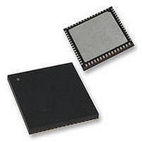
32kB Flash, 2kB RAM, 1kB EE, NanoWatt XLP, LCD 64 QFN 9x9x0.9mm TUBE
Manufacturer
Microchip Technology
Series
PIC® XLP™ 18Fr
Datasheet
1.PIC18F65K90-IMR.pdf
(570 pages)
Specifications of PIC18F65K90-I/MR
Processor Series
PIC18F
Core
PIC
Data Bus Width
8 bit
Program Memory Type
Flash
Program Memory Size
32 KB
Data Ram Size
2 KB
Interface Type
I2C, SPI
Maximum Clock Frequency
64 MHz
Number Of Timers
8
Operating Supply Voltage
1.8 V to 5.5 V
Maximum Operating Temperature
+ 125 C
3rd Party Development Tools
52715-96, 52716-328, 52717-734, 52712-325, EWPIC18
Minimum Operating Temperature
- 40 C
On-chip Adc
12 bit, 16 Channel
Core Processor
PIC
Core Size
8-Bit
Speed
64MHz
Connectivity
I²C, LIN, SPI, UART/USART
Peripherals
Brown-out Detect/Reset, LCD, POR, PWM, WDT
Number Of I /o
53
Eeprom Size
1K x 8
Ram Size
2K x 8
Voltage - Supply (vcc/vdd)
1.8 V ~ 5.5 V
Data Converters
A/D 16x12b
Oscillator Type
Internal
Operating Temperature
-40°C ~ 85°C
Package / Case
64-VFQFN Exposed Pad
Lead Free Status / Rohs Status
Details


19.4.2.1
In the Full-Bridge mode, the PxM1 bit in the CCPxCON
register allows users to control the forward/reverse
direction. When the application firmware changes this
direction control bit, the module will change to the new
direction on the next PWM cycle.
A direction change is initiated in software by changing
the PxM1 bit of the CCPxCON register. The following
sequence occurs prior to the end of the current PWM
period:
• The modulated outputs (PxB and PxD) are placed
• The associated unmodulated outputs (PxA and
• PWM modulation resumes at the beginning of the
For an illustration of this sequence, see
The Full-Bridge mode does not provide a dead-band
delay. As one output is modulated at a time, a
dead-band delay is generally not required. There is a
situation where a dead-band delay is required. This
situation occurs when both of the following conditions
are true:
FIGURE 19-10:
2009-2011 Microchip Technology Inc.
in their inactive state.
PxC) are switched to drive in the opposite
direction.
next period.
Note 1: The direction bit, PxM1 of the CCPxCON register, is written any time during the PWM cycle.
PxA (Active-High)
PxB (Active-High)
PxC (Active-High)
PxD (Active-High)
2: When changing directions, the PxA and PxC signals switch before the end of the current PWM cycle. The
Direction Change in Full-Bridge Mode
modulated PxB and PxD signals are inactive at this time. The length of this time is:
(1/F
Signal
OSC
EXAMPLE OF PWM DIRECTION CHANGE
) • TMR2 Prescale Value.
Pulse Width
Figure
Period
19-10.
(1)
PIC18F87K90 FAMILY
• The direction of the PWM output changes when
• The turn-off time of the power switch, including
Figure 19-11
changing from forward to reverse, at a near 100% duty
cycle. In this example, at time, t1, the PxA and PxD
outputs become inactive, while the PxC output
becomes active. Since the turn-off time of the power
devices is longer than the turn-on time, a shoot-through
current will flow through power devices, QC and QD
(see
phenomenon will occur to power devices, QA and QB,
for PWM direction change from reverse to forward.
If changing PWM direction at high duty cycle is required
for an application, two possible solutions for eliminating
the shoot-through current are:
• Reduce PWM duty cycle for one PWM period
• Use switch drivers that can drive the switches off
Other options to prevent shoot-through current may
exist.
the duty cycle of the output is at or near 100%.
the power device and driver circuit, is greater than
the turn-on time.
before changing directions.
faster than they can drive them on.
Figure
Pulse Width
(2)
19-8), for the duration of ‘t’. The same
shows an example of the PWM direction
Period
DS39957D-page 263
Related parts for PIC18F65K90-I/MR
Image
Part Number
Description
Manufacturer
Datasheet
Request
R

Part Number:
Description:
Manufacturer:
Microchip Technology Inc.
Datasheet:
Part Number:
Description:
Manufacturer:
Microchip Technology Inc.
Datasheet:
Part Number:
Description:
Manufacturer:
Microchip Technology Inc.
Datasheet:
Part Number:
Description:
Manufacturer:
Microchip Technology Inc.
Datasheet:
Part Number:
Description:
Manufacturer:
Microchip Technology Inc.
Datasheet:
Part Number:
Description:
Manufacturer:
Microchip Technology Inc.
Datasheet:
Part Number:
Description:
Manufacturer:
Microchip Technology Inc.
Datasheet:
Part Number:
Description:
Manufacturer:
Microchip Technology Inc.
Datasheet: