PIC18F65K90-I/MR Microchip Technology, PIC18F65K90-I/MR Datasheet - Page 252
PIC18F65K90-I/MR
Manufacturer Part Number
PIC18F65K90-I/MR
Description
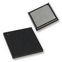
32kB Flash, 2kB RAM, 1kB EE, NanoWatt XLP, LCD 64 QFN 9x9x0.9mm TUBE
Manufacturer
Microchip Technology
Series
PIC® XLP™ 18Fr
Datasheet
1.PIC18F65K90-IMR.pdf
(570 pages)
Specifications of PIC18F65K90-I/MR
Processor Series
PIC18F
Core
PIC
Data Bus Width
8 bit
Program Memory Type
Flash
Program Memory Size
32 KB
Data Ram Size
2 KB
Interface Type
I2C, SPI
Maximum Clock Frequency
64 MHz
Number Of Timers
8
Operating Supply Voltage
1.8 V to 5.5 V
Maximum Operating Temperature
+ 125 C
3rd Party Development Tools
52715-96, 52716-328, 52717-734, 52712-325, EWPIC18
Minimum Operating Temperature
- 40 C
On-chip Adc
12 bit, 16 Channel
Core Processor
PIC
Core Size
8-Bit
Speed
64MHz
Connectivity
I²C, LIN, SPI, UART/USART
Peripherals
Brown-out Detect/Reset, LCD, POR, PWM, WDT
Number Of I /o
53
Eeprom Size
1K x 8
Ram Size
2K x 8
Voltage - Supply (vcc/vdd)
1.8 V ~ 5.5 V
Data Converters
A/D 16x12b
Oscillator Type
Internal
Operating Temperature
-40°C ~ 85°C
Package / Case
64-VFQFN Exposed Pad
Lead Free Status / Rohs Status
Details


PIC18F87K90 FAMILY
REGISTER 19-1:
DS39957D-page 252
bit 7
Legend:
R = Readable bit
-n = Value at POR
bit 7-6
bit 5-4
bit 3-0
R/W-0
PxM1
PxM<1:0>: Enhanced PWM Output Configuration bits
If CCPxM<3:2> = 00, 01, 10:
xx = PxA is assigned as a capture/compare input/output; PxB, PxC and PxD are assigned as PORT pins
If CCPxM<3:2> = 11:
00 = Single output: PxA, PxB, PxC and PxD are controlled by steering (see
01 = Full-bridge output forward: PxD is modulated; PxA is active; PxB, PxC are inactive
10 = Half-bridge output: PxA, PxB are modulated with dead-band control; PxC and PxD are
11 = Full-bridge output reverse: PxB is modulated; PxC is active; PxA and PxD are inactive
DCxB<1:0>: PWM Duty Cycle Bit 1 and Bit 0
Capture mode:
Unused.
Compare mode:
Unused.
PWM mode:
These bits are the two LSbs of the 10-bit PWM duty cycle. The eight MSbs of the duty cycle are found
in CCPRxL.
CCPxM<3:0>: ECCPx Mode Select bits
0000 = Capture/Compare/PWM off (resets ECCPx module)
0001 = Reserved
0010 = Compare mode: toggle output on match
0011 = Capture mode
0100 = Capture mode: every falling edge
0101 = Capture mode: every rising edge
0110 = Capture mode: every fourth rising edge
0111 = Capture mode: every 16
1000 = Compare mode: initialize the ECCPx pin low; set the output on a compare match (set CCPxIF)
1001 = Compare mode: initialize the ECCPx pin high; clear the output on a compare match (set CCPxIF)
1010 = Compare mode: generate a software interrupt only; ECCPx pin reverts to an I/O state
1011 = Compare mode: trigger special event (ECCPx resets TMR1 or TMR3, starts A/D conversion,
1100 = PWM mode: PxA and PxC are active-high; PxB and PxD are active-high
1101 = PWM mode: PxA and PxC are active-high; PxB and PxD are active-low
1110 = PWM mode: PxA and PxC are active-low; PxB and PxD are active-high
1111 = PWM mode: PxA and PxC are active-low; PxB and PxD are active-low
R/W-0
PxM0
Steering
assigned as PORT pins
CCPxCON: ENHANCED CAPTURE/COMPARE/PWM x CONTROL
sets CCxIF bit)
W = Writable bit
‘1’ = Bit is set
Mode”)
DCxB1
R/W-0
DCxB0
R/W-0
th
rising edge
U = Unimplemented bit, read as ‘0’
‘0’ = Bit is cleared
CCPxM3
R/W-0
CCPxM2
R/W-0
2009-2011 Microchip Technology Inc.
x = Bit is unknown
CCPxM1
R/W-0
Section 19.4.7 “Pulse
CCPxM0
R/W-0
bit 0
Related parts for PIC18F65K90-I/MR
Image
Part Number
Description
Manufacturer
Datasheet
Request
R

Part Number:
Description:
Manufacturer:
Microchip Technology Inc.
Datasheet:
Part Number:
Description:
Manufacturer:
Microchip Technology Inc.
Datasheet:
Part Number:
Description:
Manufacturer:
Microchip Technology Inc.
Datasheet:
Part Number:
Description:
Manufacturer:
Microchip Technology Inc.
Datasheet:
Part Number:
Description:
Manufacturer:
Microchip Technology Inc.
Datasheet:
Part Number:
Description:
Manufacturer:
Microchip Technology Inc.
Datasheet:
Part Number:
Description:
Manufacturer:
Microchip Technology Inc.
Datasheet:
Part Number:
Description:
Manufacturer:
Microchip Technology Inc.
Datasheet: