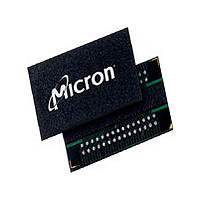
MT47H32M8BP-3:B Micron Technology Inc, MT47H32M8BP-3:B Datasheet - Page 112

MT47H32M8BP-3:B
Manufacturer Part Number
MT47H32M8BP-3:B
Description
Manufacturer
Micron Technology Inc
Type
DDR2 SDRAMr
Datasheet
1.MT47H32M8BP-3B.pdf
(128 pages)
Specifications of MT47H32M8BP-3:B
Organization
32Mx8
Density
256Mb
Address Bus
15b
Access Time (max)
450ps
Maximum Clock Rate
667MHz
Operating Supply Voltage (typ)
1.8V
Package Type
FBGA
Operating Temp Range
0C to 85C
Operating Supply Voltage (max)
1.9V
Operating Supply Voltage (min)
1.7V
Supply Current
190mA
Pin Count
60
Mounting
Surface Mount
Operating Temperature Classification
Commercial
Lead Free Status / Rohs Status
Compliant
Available stocks
Company
Part Number
Manufacturer
Quantity
Price
Company:
Part Number:
MT47H32M8BP-3:B
Manufacturer:
MICRON
Quantity:
586
Company:
Part Number:
MT47H32M8BP-3:B TR
Manufacturer:
Micron Technology Inc
Quantity:
10 000
Power-Down Mode
PDF: 09005aef8117c187
256MbDDR2.pdf - Rev. M 7/09 EN
DDR2 SDRAM supports multiple power-down modes that allow significant power sav-
ings over normal operating modes. CKE is used to enter and exit different power-down
modes. Power-down entry and exit timings are shown in Figure 68 (page 113). Detailed
power-down entry conditions are shown in Figure 69 (page 115)–Figure 76 (page 118).
Table 43 (page 114) is the CKE Truth Table.
DDR2 SDRAM requires CKE to be registered HIGH (active) at all times that an access is
in progress—from the issuing of a READ or WRITE command until completion of the
burst. Thus, a clock suspend is not supported. For READs, a burst completion is defined
when the read postamble is satisfied; for WRITEs, a burst completion is defined when
the write postamble and
READ command) are satisfied, as shown in Figure 71 (page 116) and Figure 72
(page 116) on Figure 72 (page 116). The number of clock cycles required to meet
is either two or
Power-down mode (see Figure 68 (page 113)) is entered when CKE is registered low
coincident with an NOP or DESELECT command. CKE is not allowed to go LOW during
a mode register or extended mode register command time, or while a READ or WRITE
operation is in progress. If power-down occurs when all banks are idle, this mode is
referred to as precharge power-down. If power-down occurs when there is a row active
in any bank, this mode is referred to as active power-down. Entering power-down deac-
tivates the input and output buffers, excluding CK, CK#, ODT, and CKE. For maximum
power savings, the DLL is frozen during precharge power-down. Exiting active power-
down requires the device to be at the same voltage and frequency as when it entered
power-down. Exiting precharge power-down requires the device to be at the same volt-
age as when it entered power-down; however, the clock frequency is allowed to change
(see Precharge Power-Down Clock Frequency Change (page 119)).
The maximum duration for either active or precharge power-down is limited by the re-
fresh requirements of the device
entry and exit is limited by the
tained while in power-down mode: CKE LOW, a stable clock signal, and stable power
supply signals at the inputs of the DDR2 SDRAM. All other input signals are “Don’t
Care” except ODT. Detailed ODT timing diagrams for different power-down modes are
shown in Figure 81 (page 124)–Figure 86 (page 128).
The power-down state is synchronously exited when CKE is registered HIGH (in con-
junction with a NOP or DESELECT command), as shown in Figure 68 (page 113).
t
WTR/
t
CK, whichever is greater.
t
WR (WRITE-to-PRECHARGE command) or
112
t
CKE (MIN) parameter. The following must be main-
t
RFC (MAX). The minimum duration for power-down
Micron Technology, Inc. reserves the right to change products or specifications without notice.
256Mb: x4, x8, x16 DDR2 SDRAM
Power-Down Mode
©2003 Micron Technology, Inc. All rights reserved.
t
WTR (WRITE-to-
t
WTR


