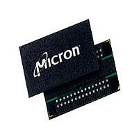
MT47H32M8BP-3:B Micron Technology Inc, MT47H32M8BP-3:B Datasheet - Page 76

MT47H32M8BP-3:B
Manufacturer Part Number
MT47H32M8BP-3:B
Description
Manufacturer
Micron Technology Inc
Type
DDR2 SDRAMr
Datasheet
1.MT47H32M8BP-3B.pdf
(128 pages)
Specifications of MT47H32M8BP-3:B
Organization
32Mx8
Density
256Mb
Address Bus
15b
Access Time (max)
450ps
Maximum Clock Rate
667MHz
Operating Supply Voltage (typ)
1.8V
Package Type
FBGA
Operating Temp Range
0C to 85C
Operating Supply Voltage (max)
1.9V
Operating Supply Voltage (min)
1.7V
Supply Current
190mA
Pin Count
60
Mounting
Surface Mount
Operating Temperature Classification
Commercial
Lead Free Status / Rohs Status
Compliant
Available stocks
Company
Part Number
Manufacturer
Quantity
Price
Company:
Part Number:
MT47H32M8BP-3:B
Manufacturer:
MICRON
Quantity:
586
Company:
Part Number:
MT47H32M8BP-3:B TR
Manufacturer:
Micron Technology Inc
Quantity:
10 000
DLL Enable/Disable
Output Drive Strength
DQS# Enable/Disable
RDQS Enable/Disable
Output Enable/Disable
PDF: 09005aef8117c187
256MbDDR2.pdf - Rev. M 7/09 EN
The DLL may be enabled or disabled by programming bit E0 during the LM command,
as shown in Figure 36 (page 75). These specifications are applicable when the DLL is
enabled for normal operation. DLL enable is required during power-up initialization
and upon returning to normal operation after having disabled the DLL for the purpose
of debugging or evaluation. Enabling the DLL should always be followed by resetting
the DLL using the LM command.
The DLL is automatically disabled when entering SELF REFRESH operation and is auto-
matically re-enabled and reset upon exit of SELF REFRESH operation.
Anytime the DLL is enabled (and subsequently reset), 200 clock cycles must occur be-
fore a READ command can be issued to allow time for the internal clock to synchronize
with the external clock. Failing to wait for synchronization to occur may result in a viola-
tion of the
Anytime the DLL is disabled and the device is operated below 25 MHz, any AUTO RE-
FRESH command should be followed by a PRECHARGE ALL command.
The output drive strength is defined by bit E1, as shown in Figure 36. The normal drive
strength for all outputs is specified to be SSTL_18. Programming bit E1 = 0 selects nor-
mal (full strength) drive strength for all outputs. Selecting a reduced drive strength
option (E1 = 1) will reduce all outputs to approximately 45 to 60 percent of the SSTL_18
drive strength. This option is intended for the support of lighter load and/or point-to-
point environments.
The DQS# ball is enabled by bit E10. When E10 = 0, DQS# is the complement of the
differential data strobe pair DQS/DQS#. When disabled (E10 = 1), DQS is used in a single-
ended mode and the DQS# ball is disabled. When disabled, DQS# should be left float-
ing; however, it may be tied to ground via a 20Ω to 10kΩ resistor. This function is also
used to enable/disable RDQS#. If RDQS is enabled (E11 = 1) and DQS# is enabled (E10 =
0), then both DQS# and RDQS# will be enabled.
The RDQS ball is enabled by bit E11, as shown in Figure 36. This feature is only applica-
ble to the x8 configuration. When enabled (E11 = 1), RDQS is identical in function and
timing to data strobe DQS during a READ. During a WRITE operation, RDQS is ignored
by the DDR2 SDRAM.
The OUTPUT ENABLE function is defined by bit E12, as shown in Figure 36. When ena-
bled (E12 = 0), all outputs (DQ, DQS, DQS#, RDQS, RDQS#) function normally. When
disabled (E12 = 1), all outputs (DQ, DQS, DQS#, RDQS, RDQS#) are disabled, thus remov-
ing output buffer current. The output disable feature is intended to be used during I
characterization of read current.
t
AC or
t
DQSCK parameters.
76
Micron Technology, Inc. reserves the right to change products or specifications without notice.
256Mb: x4, x8, x16 DDR2 SDRAM
Extended Mode Register (EMR)
©2003 Micron Technology, Inc. All rights reserved.
DD


