EPM240GM100C5N Altera, EPM240GM100C5N Datasheet - Page 36
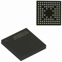
EPM240GM100C5N
Manufacturer Part Number
EPM240GM100C5N
Description
IC MAX II CPLD 240 LE 100-MBGA
Manufacturer
Altera
Series
MAX® IIr
Datasheets
1.EPM240GT100C5N.pdf
(6 pages)
2.EPM240GT100C5N.pdf
(88 pages)
3.EPM240GM100C5N.pdf
(10 pages)
Specifications of EPM240GM100C5N
Programmable Type
In System Programmable
Delay Time Tpd(1) Max
4.7ns
Voltage Supply - Internal
1.71 V ~ 1.89 V
Number Of Logic Elements/blocks
240
Number Of Macrocells
192
Number Of I /o
80
Operating Temperature
0°C ~ 85°C
Mounting Type
Surface Mount
Package / Case
100-MBGA
Voltage
1.8V
Memory Type
FLASH
Number Of Logic Elements/cells
240
Family Name
MAX II
# Macrocells
192
Frequency (max)
1.8797GHz
Propagation Delay Time
7.5ns
Number Of Logic Blocks/elements
24
# I/os (max)
80
Operating Supply Voltage (typ)
1.8V
In System Programmable
Yes
Operating Supply Voltage (min)
1.71V
Operating Supply Voltage (max)
1.89V
Operating Temp Range
0C to 85C
Operating Temperature Classification
Commercial
Mounting
Surface Mount
Pin Count
100
Package Type
MBGA
Lead Free Status / RoHS Status
Lead free / RoHS Compliant
Features
-
Lead Free Status / Rohs Status
Compliant
Other names
544-1726
Available stocks
Company
Part Number
Manufacturer
Quantity
Price
Company:

Part Number:
EPM240GM100C5N
Manufacturer:
CYPESS
Quantity:
1
Company:
Part Number:
EPM240GM100C5N
Manufacturer:
ALTERA10
Quantity:
1 287
Part Number:
EPM240GM100C5N
Manufacturer:
ALTERA/阿尔特拉
Quantity:
20 000


2–28
Figure 2–23. MAX II I/O Banks for EPM1270 and EPM2210
Notes to
(1)
(2)
MAX II Device Handbook
Figure 2–23
Figure 2–23
Figure
2–23:
is a top view of the silicon die.
is a graphical representation only. Refer to the pin list and the Quartus II software for exact pin locations.
I/O Bank 1
Each I/O bank has dedicated V
in that bank. A single device can support 1.5-V, 1.8-V, 2.5-V, and 3.3-V interfaces; each
individual bank can support a different standard. Each I/O bank can support
multiple standards with the same V
V
the input and output buffers in MAX II devices.
The JTAG pins for MAX II devices are dedicated pins that cannot be used as regular
I/O pins. The pins TMS, TDI, TDO, and TCK support all the I/O standards shown in
Table 2–4 on page 2–27
devices and their I/O standard support is controlled by the V
PCI Compliance
The MAX II EPM1270 and EPM2210 devices are compliant with PCI applications as
well as all 3.3-V electrical specifications in the PCI Local Bus Specification Revision 2.2.
These devices are also large enough to support PCI intellectual property (IP) cores.
Table 2–5
specifications.
CCIO
is 3.3 V, Bank 3 can support LVTTL, LVCMOS, and 3.3-V PCI. V
shows the MAX II device speed grades that meet the PCI timing
All I/O Banks Support
■
■
■
■
except for PCI. These pins reside in Bank 1 for all MAX II
3.3-V LVTTL/LVCMOS
2.5-V LVTTL/LVCMOS
1.8-V LVTTL/LVCMOS
1.5-V LVCMOS
I/O Bank 2
I/O Bank 4
CCIO
(Note
pins that determine the voltage standard support
CCIO
1),
for input and output pins. For example, when
(2)
© October 2008 Altera Corporation
I/O Bank 3
CCIO
Also Supports
the 3.3-V PCI
I/O Standard
Chapter 2: MAX II Architecture
setting for Bank 1.
CCIO
powers both
I/O Structure
Related parts for EPM240GM100C5N
Image
Part Number
Description
Manufacturer
Datasheet
Request
R

Part Number:
Description:
CYCLONE II STARTER KIT EP2C20N
Manufacturer:
Altera
Datasheet:


Part Number:
Description:
CPLD, EP610 Family, ECMOS Process, 300 Gates, 16 Macro Cells, 16 Reg., 16 User I/Os, 5V Supply, 35 Speed Grade, 24DIP
Manufacturer:
Altera Corporation
Datasheet:
Part Number:
Description:
CPLD, EP610 Family, ECMOS Process, 300 Gates, 16 Macro Cells, 16 Reg., 16 User I/Os, 5V Supply, 15 Speed Grade, 24DIP
Manufacturer:
Altera Corporation
Datasheet:
Part Number:
Description:
Manufacturer:
Altera Corporation
Datasheet:
Part Number:
Description:
CPLD, EP610 Family, ECMOS Process, 300 Gates, 16 Macro Cells, 16 Reg., 16 User I/Os, 5V Supply, 30 Speed Grade, 24DIP
Manufacturer:
Altera Corporation
Datasheet:
Part Number:
Description:
High-performance, low-power erasable programmable logic devices with 8 macrocells, 10ns
Manufacturer:
Altera Corporation
Datasheet:
Part Number:
Description:
High-performance, low-power erasable programmable logic devices with 8 macrocells, 7ns
Manufacturer:
Altera Corporation
Datasheet:
Part Number:
Description:
Classic EPLD
Manufacturer:
Altera Corporation
Datasheet:
Part Number:
Description:
High-performance, low-power erasable programmable logic devices with 8 macrocells, 10ns
Manufacturer:
Altera Corporation
Datasheet:
Part Number:
Description:
Manufacturer:
Altera Corporation
Datasheet:
Part Number:
Description:
Manufacturer:
Altera Corporation
Datasheet:
Part Number:
Description:
Manufacturer:
Altera Corporation
Datasheet:
Part Number:
Description:
CPLD, EP610 Family, ECMOS Process, 300 Gates, 16 Macro Cells, 16 Reg., 16 User I/Os, 5V Supply, 25 Speed Grade, 24DIP
Manufacturer:
Altera Corporation
Datasheet: