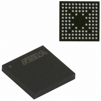
EPM240GM100C5N Altera, EPM240GM100C5N Datasheet - Page 67

EPM240GM100C5N
Manufacturer Part Number
EPM240GM100C5N
Description
IC MAX II CPLD 240 LE 100-MBGA
Manufacturer
Altera
Series
MAX® IIr
Datasheets
1.EPM240GT100C5N.pdf
(6 pages)
2.EPM240GT100C5N.pdf
(88 pages)
3.EPM240GM100C5N.pdf
(10 pages)
Specifications of EPM240GM100C5N
Programmable Type
In System Programmable
Delay Time Tpd(1) Max
4.7ns
Voltage Supply - Internal
1.71 V ~ 1.89 V
Number Of Logic Elements/blocks
240
Number Of Macrocells
192
Number Of I /o
80
Operating Temperature
0°C ~ 85°C
Mounting Type
Surface Mount
Package / Case
100-MBGA
Voltage
1.8V
Memory Type
FLASH
Number Of Logic Elements/cells
240
Family Name
MAX II
# Macrocells
192
Frequency (max)
1.8797GHz
Propagation Delay Time
7.5ns
Number Of Logic Blocks/elements
24
# I/os (max)
80
Operating Supply Voltage (typ)
1.8V
In System Programmable
Yes
Operating Supply Voltage (min)
1.71V
Operating Supply Voltage (max)
1.89V
Operating Temp Range
0C to 85C
Operating Temperature Classification
Commercial
Mounting
Surface Mount
Pin Count
100
Package Type
MBGA
Lead Free Status / RoHS Status
Lead free / RoHS Compliant
Features
-
Lead Free Status / Rohs Status
Compliant
Other names
544-1726
Available stocks
Company
Part Number
Manufacturer
Quantity
Price
Company:
Part Number:
EPM240GM100C5N
Manufacturer:
CYPESS
Quantity:
1
Company:
Part Number:
EPM240GM100C5N
Manufacturer:
ALTERA10
Quantity:
1 287
Part Number:
EPM240GM100C5N
Manufacturer:
ALTERA/阿尔特拉
Quantity:
20 000
Chapter 5: DC and Switching Characteristics
Timing Model and Specifications
Figure 5–2. MAX II Device Timing Model
Preliminary and Final Timing
© August 2009 Altera Corporation
I/O Pin
INPUT
I/O Input Delay
f
t
IN
The timing characteristics of any signal path can be derived from the timing model
and parameters of a particular device. External timing parameters, which represent
pin-to-pin timing delays, can be calculated as the sum of internal parameters.
Refer to the
Handbook for more information.
This section describes and specifies the performance, internal, external, and UFM
timing specifications. All specifications are representative of the worst-case supply
voltage and junction temperature conditions.
Timing models can have either preliminary or final status. The Quartus II software
issues an informational message during the design compilation if the timing models
are preliminary.
Preliminary status means the timing model is subject to change. Initially, timing
numbers are created using simulation results, process data, and other known
parameters. These tests are used to make the preliminary numbers as close to the
actual timing parameters as possible.
Final timing numbers are based on actual device operation and testing. These
numbers reflect the actual performance of the device under the worst-case voltage
and junction temperature conditions.
Table 5–13. MAX II Device Timing Model Status
EPM240
EPM240Z
EPM570
EPM570Z
Input Routing
Global Input Delay
Memory
Delay
Flash
User
t
DL
t
GLOB
Device
(1)
(1)
Data-In/LUT Chain
Understanding Timing in MAX II Devices
Table 5–13
To Adjacent LE
Register Control
LUT Delay
t
Logic Element
Delay
LUT
t
C
t
R4
shows the status of the MAX II device timing models.
Preliminary
t
COMB
t
t
t
—
—
—
—
t
PRE
CLR
CO
SU
t
H
Register Delays
t
C4
(Part 1 of 2)
Data-Out
Combinational Path Delay
From Adjacent LE
Output Routing
chapter in the MAX II Device
Final
v
v
v
v
t
Delay
FASTIO
t
IODR
t
IOE
Output and Output Enable
Data Delay
Output
Delay
t
t
t
OD
XZ
MAX II Device Handbook
ZX
I/O Pin
5–9


