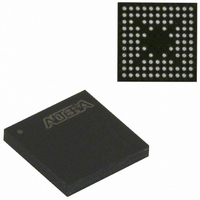
EPM240GM100C5N Altera, EPM240GM100C5N Datasheet - Page 79

EPM240GM100C5N
Manufacturer Part Number
EPM240GM100C5N
Description
IC MAX II CPLD 240 LE 100-MBGA
Manufacturer
Altera
Series
MAX® IIr
Datasheets
1.EPM240GT100C5N.pdf
(6 pages)
2.EPM240GT100C5N.pdf
(88 pages)
3.EPM240GM100C5N.pdf
(10 pages)
Specifications of EPM240GM100C5N
Programmable Type
In System Programmable
Delay Time Tpd(1) Max
4.7ns
Voltage Supply - Internal
1.71 V ~ 1.89 V
Number Of Logic Elements/blocks
240
Number Of Macrocells
192
Number Of I /o
80
Operating Temperature
0°C ~ 85°C
Mounting Type
Surface Mount
Package / Case
100-MBGA
Voltage
1.8V
Memory Type
FLASH
Number Of Logic Elements/cells
240
Family Name
MAX II
# Macrocells
192
Frequency (max)
1.8797GHz
Propagation Delay Time
7.5ns
Number Of Logic Blocks/elements
24
# I/os (max)
80
Operating Supply Voltage (typ)
1.8V
In System Programmable
Yes
Operating Supply Voltage (min)
1.71V
Operating Supply Voltage (max)
1.89V
Operating Temp Range
0C to 85C
Operating Temperature Classification
Commercial
Mounting
Surface Mount
Pin Count
100
Package Type
MBGA
Lead Free Status / RoHS Status
Lead free / RoHS Compliant
Features
-
Lead Free Status / Rohs Status
Compliant
Other names
544-1726
Available stocks
Company
Part Number
Manufacturer
Quantity
Price
Company:
Part Number:
EPM240GM100C5N
Manufacturer:
CYPESS
Quantity:
1
Company:
Part Number:
EPM240GM100C5N
Manufacturer:
ALTERA10
Quantity:
1 287
Part Number:
EPM240GM100C5N
Manufacturer:
ALTERA/阿尔特拉
Quantity:
20 000
Chapter 5: DC and Switching Characteristics
Timing Model and Specifications
Table 5–26. EPM2210 Global Clock External I/O Timing Parameters
External Timing I/O Delay Adders
Table 5–27. External Timing Input Delay Adders (Part 1 of 2)
© August 2009 Altera Corporation
t
t
t
t
t
t
t
t
f
Note to
(1) The maximum frequency is limited by the I/O standard on the clock input pin. The 16-bit counter critical delay performs faster than this global
3.3-V LVTTL
PD1
PD2
SU
H
CO
CH
CL
CNT
CNT
Symbol
clock input pin maximum frequency.
Table
I/O Standard
5–26:
Worst case pin-to-pin delay
through 1 look-up table
(LUT)
Best case pin-to-pin delay
through 1 LUT
Global clock setup time
Global clock hold time
Global clock to output delay
Global clock high time
Global clock low time
Minimum global clock
period for
16-bit counter
Maximum global clock
frequency for 16-bit counter
Without Schmitt
Trigger
With Schmitt
Trigger
Table 5–26
The I/O delay timing parameters for I/O standard input and output adders, and
input delays are specified by speed grade independent of device density.
Table 5–27
packages. The delay numbers for –3, –4, and –5 speed grades shown in
through
grade values are based on an EPM570Z device target. If an I/O standard other than
3.3-V LVTTL is selected, add the input delay adder to the external t
parameters shown in
3.3-V LVTTL with 16 mA drive strength and fast slew rate is selected, add the output
delay adder to the external t
Parameter
Table 5–33
shows the external I/O timing parameters for EPM2210 devices.
through
Min
—
—
–3 Speed
Grade
Max
334
0
Condition
are based on an EPM1270 device target, while –6, –7, and –8 speed
Table 5–31
10 pF
10 pF
10 pF
MAX II / MAX IIG
Table 5–23
—
—
—
—
—
—
Min
—
—
–4 Speed
Grade
CO
Max Min
434
–3 Speed Grade
0
show the adder delays associated with I/O pins for all
and t
Min
166
166
1.2
2.0
3.3
—
—
—
0
through
—
—
PD
–5 Speed
Grade
shown in
304.0
Max
7.0
3.7
4.6
(1)
—
—
—
—
—
Max
535
Table
0
MAX II / MAX IIG
–4 Speed Grade
Min Max
5–26. If an I/O standard other than
Min
216
216
—
—
1.5
2.0
4.0
–6 Speed
Table 5–23
—
—
—
0
Grade
387
0
247.5
Max
9.1
4.8
6.0
—
—
—
—
—
through
Min
—
—
–7 Speed
MAX IIZ
Grade
–5 Speed Grade
Min
266
266
1.9
2.0
5.0
—
—
—
Max
434
0
0
SU
Table
MAX II Device Handbook
timing
Min
Table 5–27
201.1
—
—
–8 Speed
Max
11.2
5.9
7.4
—
—
—
—
—
Grade
5–26.
Max
442
0
MHz
Unit
ns
ns
ns
ns
ns
ps
ps
ns
5–21
Unit
ps
ps


