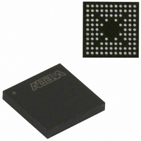
EPM240GM100C5N Altera, EPM240GM100C5N Datasheet - Page 56

EPM240GM100C5N
Manufacturer Part Number
EPM240GM100C5N
Description
IC MAX II CPLD 240 LE 100-MBGA
Manufacturer
Altera
Series
MAX® IIr
Datasheets
1.EPM240GT100C5N.pdf
(6 pages)
2.EPM240GT100C5N.pdf
(88 pages)
3.EPM240GM100C5N.pdf
(10 pages)
Specifications of EPM240GM100C5N
Programmable Type
In System Programmable
Delay Time Tpd(1) Max
4.7ns
Voltage Supply - Internal
1.71 V ~ 1.89 V
Number Of Logic Elements/blocks
240
Number Of Macrocells
192
Number Of I /o
80
Operating Temperature
0°C ~ 85°C
Mounting Type
Surface Mount
Package / Case
100-MBGA
Voltage
1.8V
Memory Type
FLASH
Number Of Logic Elements/cells
240
Family Name
MAX II
# Macrocells
192
Frequency (max)
1.8797GHz
Propagation Delay Time
7.5ns
Number Of Logic Blocks/elements
24
# I/os (max)
80
Operating Supply Voltage (typ)
1.8V
In System Programmable
Yes
Operating Supply Voltage (min)
1.71V
Operating Supply Voltage (max)
1.89V
Operating Temp Range
0C to 85C
Operating Temperature Classification
Commercial
Mounting
Surface Mount
Pin Count
100
Package Type
MBGA
Lead Free Status / RoHS Status
Lead free / RoHS Compliant
Features
-
Lead Free Status / Rohs Status
Compliant
Other names
544-1726
Available stocks
Company
Part Number
Manufacturer
Quantity
Price
Company:
Part Number:
EPM240GM100C5N
Manufacturer:
CYPESS
Quantity:
1
Company:
Part Number:
EPM240GM100C5N
Manufacturer:
ALTERA10
Quantity:
1 287
Part Number:
EPM240GM100C5N
Manufacturer:
ALTERA/阿尔特拉
Quantity:
20 000
4–6
Power-Up Characteristics
MAX II Device Handbook
1
When power is applied to a MAX II device, the POR circuit monitors V
begins SRAM download at an approximate voltage of 1.7 V or 1.55 V for MAX IIG and
MAX IIZ devices. From this voltage reference, SRAM download and entry into user
mode takes 200 to 450 µs maximum, depending on device density. This period of time
is specified as t
Characteristics
Entry into user mode is gated by whether all V
operating voltage. If V
user mode within the t
V
For MAX II and MAX IIG devices, when in user mode, the POR circuitry continues to
monitor the V
there is a V
the SRAM and tri-states the I/O pins. Once V
(or 1.55 V for MAX IIG devices), the SRAM download restarts and the device begins
to operate after t
For MAX IIZ devices, the POR circuitry does not monitor the V
levels after the device enters user mode. If there is a V
during user mode, the functionality of the device will not be guaranteed and you
must power down the V
and V
SRAM download restarts and the device begins to operate after t
passed.
Figure 4–5
during power-up into user mode and from user mode to power-down or brown-out.
All V
entering user mode.
CCINT
CCINT
, the device does not enter user mode until 2 µs after all V
CCIO
and V
up again. Once V
shows the voltages for POR of MAX II, MAX IIG, and MAX IIZ devices
CCINT
CCINT
chapter in the MAX II Device Handbook.
CONFIG
voltage sag at or below 1.4 V during user mode, the POR circuit resets
CCIO
CONFIG
(but not V
pins of all banks must be powered on MAX II devices before
in the power-up timing section of the
time has passed.
CCIN
CONFIG
CCINT
T and V
CCINT
specifications. If V
CCIO
to 0 V for a minimum of 10 µs before powering the V
rises from 0 V back to approximately 1.55 V, the
) voltage level to detect a brown-out condition. If
CCIO
are powered simultaneously, the device enters
Chapter 4: Hot Socketing and Power-On Reset in MAX II Devices
CCINT
CCIO
CCIO
rises back to approximately 1.7 V
banks are powered with sufficient
is powered more than t
CCINT
DC and Switching
voltage sag below 1.4 V
© October 2008 Altera Corporation
CCIO
CCINT
CONFIG
banks are powered.
Power-On Reset Circuitry
and V
time has
CCINT
CONFIG
CCIO
and
voltage
after
CCINT


