EPM240GM100C5N Altera, EPM240GM100C5N Datasheet - Page 70
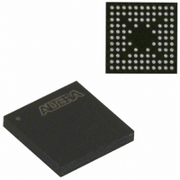
EPM240GM100C5N
Manufacturer Part Number
EPM240GM100C5N
Description
IC MAX II CPLD 240 LE 100-MBGA
Manufacturer
Altera
Series
MAX® IIr
Datasheets
1.EPM240GT100C5N.pdf
(6 pages)
2.EPM240GT100C5N.pdf
(88 pages)
3.EPM240GM100C5N.pdf
(10 pages)
Specifications of EPM240GM100C5N
Programmable Type
In System Programmable
Delay Time Tpd(1) Max
4.7ns
Voltage Supply - Internal
1.71 V ~ 1.89 V
Number Of Logic Elements/blocks
240
Number Of Macrocells
192
Number Of I /o
80
Operating Temperature
0°C ~ 85°C
Mounting Type
Surface Mount
Package / Case
100-MBGA
Voltage
1.8V
Memory Type
FLASH
Number Of Logic Elements/cells
240
Family Name
MAX II
# Macrocells
192
Frequency (max)
1.8797GHz
Propagation Delay Time
7.5ns
Number Of Logic Blocks/elements
24
# I/os (max)
80
Operating Supply Voltage (typ)
1.8V
In System Programmable
Yes
Operating Supply Voltage (min)
1.71V
Operating Supply Voltage (max)
1.89V
Operating Temp Range
0C to 85C
Operating Temperature Classification
Commercial
Mounting
Surface Mount
Pin Count
100
Package Type
MBGA
Lead Free Status / RoHS Status
Lead free / RoHS Compliant
Features
-
Lead Free Status / Rohs Status
Compliant
Other names
544-1726
Available stocks
Company
Part Number
Manufacturer
Quantity
Price
Company:

Part Number:
EPM240GM100C5N
Manufacturer:
CYPESS
Quantity:
1
Company:
Part Number:
EPM240GM100C5N
Manufacturer:
ALTERA10
Quantity:
1 287
Part Number:
EPM240GM100C5N
Manufacturer:
ALTERA/阿尔特拉
Quantity:
20 000


5–12
Table 5–16. IOE Internal Timing Microparameters
Table 5–17. t
MAX II Device Handbook
t
t
t
t
t
t
t
t
Notes to
(1) Delay numbers for t
(2) Refer to
(3) Refer to
(4) Refer to
3.3-V LVTTL
3.3-V LVCMOS
2.5-V LVTTL /
LVCMOS
1.8-V LVTTL /
LVCMOS
Symbol
FAS TIO
IN
GLOB
IOE
DL
OD
XZ
ZX
(3)
(4)
(2)
(1)
device target.
Standard
Table
Data output delay
from adjacent LE
to I/O block
I/O input pad and
buffer delay
I/O input pad and
buffer delay used
as global signal pin
Internally
generated output
enable delay
Input routing delay
Output delay buffer
and pad delay
Output buffer
disable delay
Output buffer
enable delay
Table 5–32
Table 5–19
Table 5–17
ZX
5–16:
Parameter
IOE Microparameter Adders for Fast Slew Rate
16 mA
14 mA
8 mA
8 mA
4 mA
7 mA
6 mA
3 mA
GLOB
and
and
and
Table 5–17
when using an I/O standard other than 3.3-V LVTTL with 16 mA drive strength.
differ for each device density and speed grade. The delay numbers for t
5–24
5–14
5–13
Min
—
—
—
—
—
—
—
—
–3 Speed
for delay adders associated with different I/O standards, drive strengths, and slew rates.
for t
for t
Grade
Min
—
—
—
—
—
—
—
—
XZ
ZX
–3 Speed
1,443
Max
Grade
delay adders associated with different I/O standards, drive strengths, and slew rates.
delay adders associated with different I/O standards, drive strengths, and slew rates.
314
450
28
28
14
through
0
0
1,519
1,064
1,003
Max
159
708
354
224
756
MAX II / MAX IIG
Min
—
—
—
—
—
—
—
—
MAX II / MAX IIG
–4 Speed
Grade
Table 5–20
Min
—
—
—
—
—
—
—
—
–4 Speed
1,876
Grade
Max
409
585
37
37
19
0
0
1,974
1,383
1,303
Max
207
920
374
291
982
Min
show the adder delays for t
—
—
—
—
—
—
—
—
–5 Speed
Min
Grade
—
—
–5 Speed
—
—
—
—
—
—
Grade
2,309
Max
503
720
45
45
23
(Part 1 of 2)
0
0
1,132
2,430
1,702
1,209
1,604
Max
254
460
358
Min
—
—
—
—
—
—
—
—
–6 Speed
Min
—
—
—
—
—
Grade
—
—
—
–6 Speed
Grade
Max
162
279
499
GLOB
72
72
75
2,261
1,319
1,045
1,160
0
0
Max
170
907
530
318
Chapter 5: DC and Switching Characteristics
, shown in
Min
—
—
—
—
—
—
—
—
–7 Speed
Min
MAX IIZ
ZX
—
—
—
—
—
—
—
—
Grade
–7 Speed
MAX IIZ
© August 2009 Altera Corporation
Grade
and t
Table
Max
174
289
508
Timing Model and Specifications
71
71
87
2,670
1,526
1,264
1,325
0
0
Max
348
970
966
410
5–16, are based on an EPM240
XZ
microparameters
Min
—
—
—
—
—
—
—
—
–8 Speed
Min
Grade
—
—
—
—
—
—
—
—
–8 Speed
Grade
Max
177
291
512
74
74
90
0
0
3,322
1,410
1,543
1,276
1,353
Max
428
986
509
Unit
ps
ps
ps
ps
ps
ps
ps
ps
Unit
ps
ps
ps
ps
ps
ps
ps
ps
Related parts for EPM240GM100C5N
Image
Part Number
Description
Manufacturer
Datasheet
Request
R

Part Number:
Description:
CYCLONE II STARTER KIT EP2C20N
Manufacturer:
Altera
Datasheet:


Part Number:
Description:
CPLD, EP610 Family, ECMOS Process, 300 Gates, 16 Macro Cells, 16 Reg., 16 User I/Os, 5V Supply, 35 Speed Grade, 24DIP
Manufacturer:
Altera Corporation
Datasheet:
Part Number:
Description:
CPLD, EP610 Family, ECMOS Process, 300 Gates, 16 Macro Cells, 16 Reg., 16 User I/Os, 5V Supply, 15 Speed Grade, 24DIP
Manufacturer:
Altera Corporation
Datasheet:
Part Number:
Description:
Manufacturer:
Altera Corporation
Datasheet:
Part Number:
Description:
CPLD, EP610 Family, ECMOS Process, 300 Gates, 16 Macro Cells, 16 Reg., 16 User I/Os, 5V Supply, 30 Speed Grade, 24DIP
Manufacturer:
Altera Corporation
Datasheet:
Part Number:
Description:
High-performance, low-power erasable programmable logic devices with 8 macrocells, 10ns
Manufacturer:
Altera Corporation
Datasheet:
Part Number:
Description:
High-performance, low-power erasable programmable logic devices with 8 macrocells, 7ns
Manufacturer:
Altera Corporation
Datasheet:
Part Number:
Description:
Classic EPLD
Manufacturer:
Altera Corporation
Datasheet:
Part Number:
Description:
High-performance, low-power erasable programmable logic devices with 8 macrocells, 10ns
Manufacturer:
Altera Corporation
Datasheet:
Part Number:
Description:
Manufacturer:
Altera Corporation
Datasheet:
Part Number:
Description:
Manufacturer:
Altera Corporation
Datasheet:
Part Number:
Description:
Manufacturer:
Altera Corporation
Datasheet:
Part Number:
Description:
CPLD, EP610 Family, ECMOS Process, 300 Gates, 16 Macro Cells, 16 Reg., 16 User I/Os, 5V Supply, 25 Speed Grade, 24DIP
Manufacturer:
Altera Corporation
Datasheet: