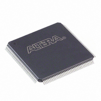
EP2C5T144I8N Altera, EP2C5T144I8N Datasheet - Page 163

EP2C5T144I8N
Manufacturer Part Number
EP2C5T144I8N
Description
IC CYCLONE II FPGA 5K 144-TQFP
Manufacturer
Altera
Series
Cyclone® IIr
Datasheet
1.EP2C5T144C8N.pdf
(168 pages)
Specifications of EP2C5T144I8N
Number Of Logic Elements/cells
4608
Number Of Labs/clbs
288
Total Ram Bits
119808
Number Of I /o
89
Voltage - Supply
1.15 V ~ 1.25 V
Mounting Type
Surface Mount
Operating Temperature
-40°C ~ 100°C
Package / Case
144-TQFP, 144-VQFP
Family Name
Cyclone® II
Number Of Logic Blocks/elements
4608
# I/os (max)
89
Frequency (max)
402.58MHz
Process Technology
90nm
Operating Supply Voltage (typ)
1.2V
Logic Cells
4608
Ram Bits
119808
Operating Supply Voltage (min)
1.15V
Operating Supply Voltage (max)
1.25V
Operating Temp Range
-40C to 100C
Operating Temperature Classification
Industrial
Mounting
Surface Mount
Pin Count
144
Package Type
TQFP
Lead Free Status / RoHS Status
Lead free / RoHS Compliant
Number Of Gates
-
Lead Free Status / Rohs Status
Compliant
Other names
544-2139
Available stocks
Company
Part Number
Manufacturer
Quantity
Price
Company:
Part Number:
EP2C5T144I8N
Manufacturer:
ALTERA41
Quantity:
710
Part Number:
EP2C5T144I8N
Manufacturer:
ALTERA/阿尔特拉
Quantity:
20 000
Altera Corporation
February 2008
The actual half period is then = 3000 ps – 155 ps = 2845 ps
Notes to
(1)
(2)
LVCMOS
LVTTL
2.5-V
1.8-V
1.5-V
SSTL-2 Class I
SSTL-2 Class II
SSTL-18 Class I
SSTL-18 Class II
HSTL-18 Class I
HSTL-18 Class II
HSTL-15 Class I
HSTL-15 Class II
Differential SSTL-2 Class I
Differential SSTL-2 Class II
Differential SSTL-18 Class I
Differential SSTL-18 Class II
Differential HSTL-18 Class I
Differential HSTL-18 Class II
Differential HSTL-15 Class I
Differential HSTL-15 Class II
LVDS
Simple RSDS
Mini-LVDS
Column I/O Pins in the Clock Path
Table 5–58. Maximum DCD for DDIO Output on Column I/O Pins with PLL in
the Clock Path
The DCD specification is characterized using the maximum drive strength
available for each I/O standard.
Numbers are applicable for commercial, industrial, and automotive devices.
Table
5–58:
Notes
(1),
(2)
DC Characteristics and Timing Specifications
Cyclone II Device Handbook, Volume 1
285
305
175
190
605
125
195
130
135
135
165
220
190
125
195
130
132
135
165
220
190
110
125
110
C6
400
405
195
205
645
210
195
240
270
240
240
335
210
210
195
240
270
240
240
335
210
120
125
120
C7
445
460
285
260
645
245
195
245
330
240
285
335
375
245
195
245
330
240
285
335
375
125
275
125
C8
Unit
ps
ps
ps
ps
ps
ps
ps
ps
ps
ps
ps
ps
ps
ps
ps
ps
ps
ps
ps
ps
ps
ps
ps
ps
5–73


