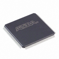
EP2C5T144I8N Altera, EP2C5T144I8N Datasheet - Page 86

EP2C5T144I8N
Manufacturer Part Number
EP2C5T144I8N
Description
IC CYCLONE II FPGA 5K 144-TQFP
Manufacturer
Altera
Series
Cyclone® IIr
Datasheet
1.EP2C5T144C8N.pdf
(168 pages)
Specifications of EP2C5T144I8N
Number Of Logic Elements/cells
4608
Number Of Labs/clbs
288
Total Ram Bits
119808
Number Of I /o
89
Voltage - Supply
1.15 V ~ 1.25 V
Mounting Type
Surface Mount
Operating Temperature
-40°C ~ 100°C
Package / Case
144-TQFP, 144-VQFP
Family Name
Cyclone® II
Number Of Logic Blocks/elements
4608
# I/os (max)
89
Frequency (max)
402.58MHz
Process Technology
90nm
Operating Supply Voltage (typ)
1.2V
Logic Cells
4608
Ram Bits
119808
Operating Supply Voltage (min)
1.15V
Operating Supply Voltage (max)
1.25V
Operating Temp Range
-40C to 100C
Operating Temperature Classification
Industrial
Mounting
Surface Mount
Pin Count
144
Package Type
TQFP
Lead Free Status / RoHS Status
Lead free / RoHS Compliant
Number Of Gates
-
Lead Free Status / Rohs Status
Compliant
Other names
544-2139
Available stocks
Company
Part Number
Manufacturer
Quantity
Price
Company:
Part Number:
EP2C5T144I8N
Manufacturer:
ALTERA41
Quantity:
710
Part Number:
EP2C5T144I8N
Manufacturer:
ALTERA/阿尔特拉
Quantity:
20 000
Hot-Socketing Feature Implementation in Cyclone II Devices
Figure 4–1. Hot-Socketing Circuit Block Diagram for Cyclone II Devices
4–4
Cyclone II Device Handbook, Volume 1
Resistor
f
Pull-Up
Weak
PAD
The POR circuit monitors V
tri-stated until the device is in user mode. The weak pull-up resistor (R)
from the I/O pin to V
tolerance control circuit permits the I/O pins to be driven by 3.3 V before
V
driving out when the device is not in user mode.
For more information, see the DC Characteristics & Timing Specifications
chapter in Volume 1 of the Cyclone II Device Handbook for the value of the
internal weak pull-up resistors.
Figure 4–2
I/O buffers. This design ensures that the output buffers do not drive
when V
than V
socketing. The V
circuit capacitance.
R
CCIO
Output
and/or V
CCIO
CCIO
. This also applies for sudden voltage spikes during hot
shows a transistor level cross section of the Cyclone II device
is powered before V
CCINT
PAD
leakage current charges the voltage tolerance control
are powered, and it prevents the I/O pins from
CCIO
Input Buffer
to Logic Array
Tolerance
Voltage
Control
keeps the I/O pins from floating. The voltage
CCINT
CCINT
Output Enable
voltage level and keeps I/O pins
or if the I/O pad voltage is higher
Hot Socket
Pre-Driver
Output
Power-On
Monitor
Reset
Altera Corporation
February 2007


