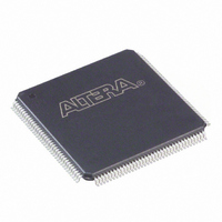
EP2C5T144I8N Altera, EP2C5T144I8N Datasheet - Page 33

EP2C5T144I8N
Manufacturer Part Number
EP2C5T144I8N
Description
IC CYCLONE II FPGA 5K 144-TQFP
Manufacturer
Altera
Series
Cyclone® IIr
Datasheet
1.EP2C5T144C8N.pdf
(168 pages)
Specifications of EP2C5T144I8N
Number Of Logic Elements/cells
4608
Number Of Labs/clbs
288
Total Ram Bits
119808
Number Of I /o
89
Voltage - Supply
1.15 V ~ 1.25 V
Mounting Type
Surface Mount
Operating Temperature
-40°C ~ 100°C
Package / Case
144-TQFP, 144-VQFP
Family Name
Cyclone® II
Number Of Logic Blocks/elements
4608
# I/os (max)
89
Frequency (max)
402.58MHz
Process Technology
90nm
Operating Supply Voltage (typ)
1.2V
Logic Cells
4608
Ram Bits
119808
Operating Supply Voltage (min)
1.15V
Operating Supply Voltage (max)
1.25V
Operating Temp Range
-40C to 100C
Operating Temperature Classification
Industrial
Mounting
Surface Mount
Pin Count
144
Package Type
TQFP
Lead Free Status / RoHS Status
Lead free / RoHS Compliant
Number Of Gates
-
Lead Free Status / Rohs Status
Compliant
Other names
544-2139
Available stocks
Company
Part Number
Manufacturer
Quantity
Price
Company:
Part Number:
EP2C5T144I8N
Manufacturer:
ALTERA41
Quantity:
710
Part Number:
EP2C5T144I8N
Manufacturer:
ALTERA/阿尔特拉
Quantity:
20 000
Altera Corporation
February 2007
Global Clock Network
The 16 or 8 global clock networks drive throughout the entire device.
Dedicated clock pins (CLK[]), PLL outputs, the logic array, and
dual-purpose clock (DPCLK[]) pins can also drive the global clock
network.
The global clock network can provide clocks for all resources within the
device, such as IOEs, LEs, memory blocks, and embedded multipliers.
The global clock lines can also be used for control signals, such as clock
enables and synchronous or asynchronous clears fed from the external
pin, or DQS signals for DDR SDRAM or QDRII SRAM interfaces. Internal
logic can also drive the global clock network for internally generated
global clocks and asynchronous clears, clock enables, or other control
signals with large fan-out.
Clock Control Block
There is a clock control block for each global clock network available in
Cyclone II devices. The clock control blocks are arranged on the device
periphery and there are a maximum of 16 clock control blocks available
per Cyclone II device. The larger Cyclone II devices (EP2C15 devices and
larger) have 16 clock control blocks, four on each side of the device. The
smaller Cyclone II devices (EP2C5 and EP2C8 devices) have eight clock
control blocks, four on the left and right sides of the device.
The control block has these functions:
■
■
In Cyclone II devices, the dedicated CLK[] pins, PLL counter outputs,
DPCLK[] pins, and internal logic can all feed the clock control block. The
output from the clock control block in turn feeds the corresponding
global clock network.
The following sources can be inputs to a given clock control block:
■
■
■
■
Dynamic global clock network clock source selection
Dynamic enable/disable of the global clock network
Four clock pins on the same side as the clock control block
Three PLL clock outputs from a PLL
Four DPCLK pins (including CDPCLK pins) on the same side as the
clock control block
Four internally-generated signals
Cyclone II Device Handbook, Volume 1
Cyclone II Architecture
2–21


