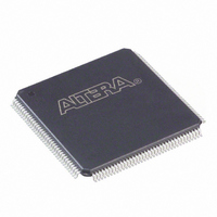
EP2C5T144I8N Altera, EP2C5T144I8N Datasheet - Page 65

EP2C5T144I8N
Manufacturer Part Number
EP2C5T144I8N
Description
IC CYCLONE II FPGA 5K 144-TQFP
Manufacturer
Altera
Series
Cyclone® IIr
Datasheet
1.EP2C5T144C8N.pdf
(168 pages)
Specifications of EP2C5T144I8N
Number Of Logic Elements/cells
4608
Number Of Labs/clbs
288
Total Ram Bits
119808
Number Of I /o
89
Voltage - Supply
1.15 V ~ 1.25 V
Mounting Type
Surface Mount
Operating Temperature
-40°C ~ 100°C
Package / Case
144-TQFP, 144-VQFP
Family Name
Cyclone® II
Number Of Logic Blocks/elements
4608
# I/os (max)
89
Frequency (max)
402.58MHz
Process Technology
90nm
Operating Supply Voltage (typ)
1.2V
Logic Cells
4608
Ram Bits
119808
Operating Supply Voltage (min)
1.15V
Operating Supply Voltage (max)
1.25V
Operating Temp Range
-40C to 100C
Operating Temperature Classification
Industrial
Mounting
Surface Mount
Pin Count
144
Package Type
TQFP
Lead Free Status / RoHS Status
Lead free / RoHS Compliant
Number Of Gates
-
Lead Free Status / Rohs Status
Compliant
Other names
544-2139
Available stocks
Company
Part Number
Manufacturer
Quantity
Price
Company:
Part Number:
EP2C5T144I8N
Manufacturer:
ALTERA41
Quantity:
710
Part Number:
EP2C5T144I8N
Manufacturer:
ALTERA/阿尔特拉
Quantity:
20 000
Altera Corporation
February 2007
Notes to
(1)
(2)
(3)
(4)
(5)
(6)
(7)
(8)
(9)
Differential HSTL-15 class I
or class II
Differential HSTL-18 class I
or class II
LVDS
RSDS and mini-LVDS
LVPECL
Table 2–17. Cyclone II Supported I/O Standards & Constraints (Part 2 of 2)
To drive inputs higher than V
LVTTL and LVCMOS input levels to overdrive input buffer option in the Quartus II software.
These pins support SSTL-18 class II and 1.8- and 1.5-V HSTL class II inputs.
PCI-X does not meet the IV curve requirement at the linear region. PCI-clamp diode is not available on top and
bottom I/O pins.
Pseudo-differential HSTL and SSTL outputs use two single-ended outputs with the second output programmed
as inverted. Pseudo-differential HSTL and SSTL inputs treat differential inputs as two single-ended HSTL and
SSTL inputs and only decode one of them.
This I/O standard is not supported on these I/O pins.
This I/O standard is only supported on the dedicated clock pins.
PLL_OUT does not support differential SSTL-18 class II and differential 1.8 and 1.5-V HSTL class II.
mini-LVDS and RSDS are only supported on output pins.
LVPECL is only supported on clock inputs.
I/O Standard
Table
(9)
2–17:
f
(8)
For more information on Cyclone II supported I/O standards, see the
Selectable I/O Standards in Cyclone II Devices chapter in Volume 1 of the
Cyclone II Device Handbook.
High-Speed Differential Interfaces
Cyclone II devices can transmit and receive data through LVDS signals at
a data rate of up to 640 Mbps and 805 Mbps, respectively. For the LVDS
transmitter and receiver, the Cyclone II device’s input and output pins
support serialization and deserialization through internal logic.
Pseudo
differential
Pseudo
differential
Differential
Differential
Differential
C C I O
Type
but less than 4.0 V, disable the PCI clamping diode and turn on the Allow
(4)
(4)
1.5 V
2.5 V
3.3 V/
2.5 V/
1.8 V/
1.5 V
Input Output
1.8 V
V
(5)
(5)
(5)
CCIO
Level
1.5 V
1.8 V
2.5 V
2.5 V
(5)
(5)
(5)
CLK,
DQS
Top & Bottom
v
v
v
v
(6)
(6)
I/O Pins
Cyclone II Device Handbook, Volume 1
User I/O
Pins
v
v
CLK,
DQS
v
(6)
v
(6)
v
v
Cyclone II Architecture
PLL_OUT
Side I/O Pins
v
v
v
v
(7)
(7)
User I/O
Pins
v
v
2–53


