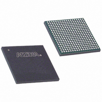
EP1C4F324C8 Altera, EP1C4F324C8 Datasheet - Page 41

EP1C4F324C8
Manufacturer Part Number
EP1C4F324C8
Description
IC CYCLONE FPGA 4K LE 324-FBGA
Manufacturer
Altera
Series
Cyclone®r
Datasheet
1.EP1C3T144C8.pdf
(106 pages)
Specifications of EP1C4F324C8
Number Of Logic Elements/cells
4000
Number Of Labs/clbs
400
Total Ram Bits
78336
Number Of I /o
249
Voltage - Supply
1.425 V ~ 1.575 V
Mounting Type
Surface Mount
Operating Temperature
0°C ~ 85°C
Package / Case
324-FBGA
Lead Free Status / RoHS Status
Contains lead / RoHS non-compliant
Number Of Gates
-
Other names
544-1044
Available stocks
Company
Part Number
Manufacturer
Quantity
Price
Company:
Part Number:
EP1C4F324C8
Manufacturer:
ALTERA
Quantity:
591
Part Number:
EP1C4F324C8
Manufacturer:
ALTERA/阿尔特拉
Quantity:
20 000
Company:
Part Number:
EP1C4F324C8N
Manufacturer:
ALTERA
Quantity:
648
Part Number:
EP1C4F324C8N
Manufacturer:
ALTERA
Quantity:
20 000
Altera Corporation
May 2008
Notes to
(1)
(2)
(3)
Dual-Purpose
Clock Pins
Table 2–7. Global Clock Network Sources (Part 2 of 2)
EP1C3 devices only have one PLL (PLL 1).
EP1C3 devices in the 100-pin TQFP package do not have dedicated clock pins CLK1 and CLK3.
EP1C3 devices in the 100-pin TQFP package do not have the DPCLK0, DPCLK1, or DPCLK5 pins.
Table
Source
2–7:
DPCLK0
DPCLK1
DPCLK2
DPCLK3
DPCLK4
DPCLK5
DPCLK6
DPCLK7
(3)
(3)
(3)
Clock Multiplication and Division
Cyclone PLLs provide clock synthesis for PLL output ports using
m/(n × post scale counter) scaling factors. The input clock is divided by
a pre-scale divider, n, and is then multiplied by the m feedback factor. The
control loop drives the VCO to match f
a unique post-scale counter to divide down the high-frequency VCO. For
multiple PLL outputs with different frequencies, the VCO is set to the
least-common multiple of the output frequencies that meets its frequency
specifications. Then, the post-scale dividers scale down the output
frequency for each output port. For example, if the output frequencies
required from one PLL are 33 and 66 MHz, the VCO is set to 330 MHz (the
least-common multiple in the VCO's range).
Each PLL has one pre-scale divider, n, that can range in value from 1 to
32. Each PLL also has one multiply divider, m, that can range in value
from 2 to 32. Global clock outputs have two post scale G dividers for
global clock outputs, and external clock outputs have an E divider for
external clock output, both ranging from 1 to 32. The Quartus II software
automatically chooses the appropriate scaling factors according to the
input frequency, multiplication, and division values entered.
GCLK0
v
—
—
—
—
—
—
—
GCLK1
v
—
—
—
—
—
—
—
GCLK2
v
—
—
—
—
—
—
—
Global Clock Network and Phase-Locked Loops
GCLK3
v
—
—
—
—
—
—
—
GCLK4
IN
v
—
—
—
—
—
—
—
× (m/n). Each output port has
GCLK5
v
—
—
—
—
—
—
—
GCLK6
v
—
—
—
—
—
—
—
Preliminary
GCLK7
v
—
—
—
—
—
—
—
2–35


