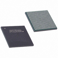
EP1C4F324C8 Altera, EP1C4F324C8 Datasheet - Page 59

EP1C4F324C8
Manufacturer Part Number
EP1C4F324C8
Description
IC CYCLONE FPGA 4K LE 324-FBGA
Manufacturer
Altera
Series
Cyclone®r
Datasheet
1.EP1C3T144C8.pdf
(106 pages)
Specifications of EP1C4F324C8
Number Of Logic Elements/cells
4000
Number Of Labs/clbs
400
Total Ram Bits
78336
Number Of I /o
249
Voltage - Supply
1.425 V ~ 1.575 V
Mounting Type
Surface Mount
Operating Temperature
0°C ~ 85°C
Package / Case
324-FBGA
Lead Free Status / RoHS Status
Contains lead / RoHS non-compliant
Number Of Gates
-
Other names
544-1044
Available stocks
Company
Part Number
Manufacturer
Quantity
Price
Company:
Part Number:
EP1C4F324C8
Manufacturer:
ALTERA
Quantity:
591
Part Number:
EP1C4F324C8
Manufacturer:
ALTERA/阿尔特拉
Quantity:
20 000
Company:
Part Number:
EP1C4F324C8N
Manufacturer:
ALTERA
Quantity:
648
Part Number:
EP1C4F324C8N
Manufacturer:
ALTERA
Quantity:
20 000
Figure 2–35. Cyclone I/O Banks
Notes to
(1)
(2)
Altera Corporation
May 2008
Also Supports
Figure 2–35
Figure 2–35
the 3.3-V PCI
I/O Standard
I/O Bank 1
Figure
I/O Bank 1
2–35:
is a top view of the silicon die.
is a graphic representation only. Refer to the pin list and the Quartus II software for exact pin locations.
and DM pins to support a DDR SDRAM or FCRAM interface. I/O bank 1
can also support a DDR SDRAM or FCRAM interface, however, the
configuration input pins in I/O bank 1 must operate at 2.5 V. I/O bank 3
can also support a DDR SDRAM or FCRAM interface, however, all the
JTAG pins in I/O bank 3 must operate at 2.5 V.
Each I/O bank has its own VCCIO pins. A single device can support 1.5-V,
1.8-V, 2.5-V, and 3.3-V interfaces; each individual bank can support a
different standard with different I/O voltages. Each bank also has
dual-purpose VREF pins to support any one of the voltage-referenced
standards (e.g., SSTL-3) independently. If an I/O bank does not use
voltage-referenced standards, the V
Notes
(1),
All I/O Banks Support
■
■
■
■
■
■
■
■
(2)
3.3-V LVTTL/LVCMOS
2.5-V LVTTL/LVCMOS
1.8-V LVTTL/LVCMOS
1.5-V LVCMOS
LVDS
RSDS
SSTL-2 Class I and II
SSTL-3 Class I and II
I/O Bank 2
I/O Bank 4
Power Bus
Individual
REF
pins are available as user I/O pins.
I/O Bank 3
I/O Bank 3
Also Supports
the 3.3-V PCI
I/O Standard
I/O Structure
Preliminary
2–53


