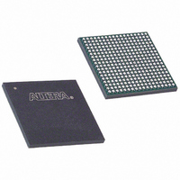
EP1C4F324C8 Altera, EP1C4F324C8 Datasheet - Page 54

EP1C4F324C8
Manufacturer Part Number
EP1C4F324C8
Description
IC CYCLONE FPGA 4K LE 324-FBGA
Manufacturer
Altera
Series
Cyclone®r
Datasheet
1.EP1C3T144C8.pdf
(106 pages)
Specifications of EP1C4F324C8
Number Of Logic Elements/cells
4000
Number Of Labs/clbs
400
Total Ram Bits
78336
Number Of I /o
249
Voltage - Supply
1.425 V ~ 1.575 V
Mounting Type
Surface Mount
Operating Temperature
0°C ~ 85°C
Package / Case
324-FBGA
Lead Free Status / RoHS Status
Contains lead / RoHS non-compliant
Number Of Gates
-
Other names
544-1044
Available stocks
Company
Part Number
Manufacturer
Quantity
Price
Company:
Part Number:
EP1C4F324C8
Manufacturer:
ALTERA
Quantity:
591
Part Number:
EP1C4F324C8
Manufacturer:
ALTERA/阿尔特拉
Quantity:
20 000
Company:
Part Number:
EP1C4F324C8N
Manufacturer:
ALTERA
Quantity:
648
Part Number:
EP1C4F324C8N
Manufacturer:
ALTERA
Quantity:
20 000
Cyclone Device Handbook, Volume 1
2–48
Preliminary
A programmable delay chain on each DQS pin allows for either a 90°
phase shift (for DDR SDRAM), or a 72° phase shift (for FCRAM) which
automatically center-aligns input DQS synchronization signals within the
data window of their corresponding DQ data signals. The phase-shifted
DQS signals drive the global clock network. This global DQS signal clocks
DQ signals on internal LE registers.
These DQS delay elements combine with the PLL’s clocking and phase
shift ability to provide a complete hardware solution for interfacing to
high-speed memory.
The clock phase shift allows the PLL to clock the DQ output enable and
output paths. The designer should use the following guidelines to meet
133 MHz performance for DDR SDRAM and FCRAM interfaces:
■
■
■
Figure 2–34
I/O through the dedicated circuitry to the logic array.
Note to
(1)
EP1C6
EP1C12
EP1C20
Table 2–10. DQ Pin Groups (Part 2 of 2)
Device
The DQS signal must be in the middle of the DQ group it clocks
Resynchronize the incoming data to the logic array clock using
successive LE registers or FIFO buffers
LE registers must be placed in the LAB adjacent to the DQ I/O pin
column it is fed by
EP1C3 devices in the 100-pin TQFP package do not have any DQ pin groups in
I/O bank 1.
Table
illustrates DDR SDRAM and FCRAM interfacing from the
2–10:
144-pin TQFP
240-pin PQFP
256-pin FineLine BGA
240-pin PQFP
256-pin FineLine BGA
324-pin FineLine BGA
324-pin FineLine BGA
400-pin FineLine BGA
Package
Number of × 8 DQ
Pin Groups
4
4
4
4
4
8
8
8
Altera Corporation
Total DQ Pin
Count
32
32
32
32
32
64
64
64
May 2008


